npj 2D Materials and Applications ( IF 9.7 ) Pub Date : 2018-08-06 , DOI: 10.1038/s41699-018-0073-3 Biswapriyo Das , Santanu Mahapatra
|
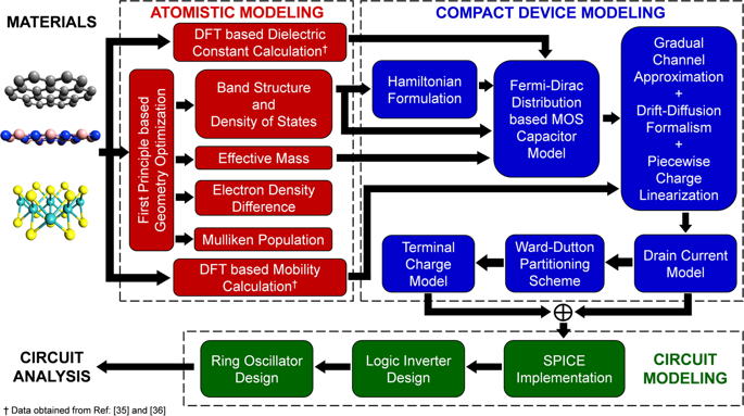
Vertical stacking of heterogeneous two-dimensional (2D) materials has received considerable attention for nanoelectronic applications. In the semiconductor industry, however, the process of integration for any new material is expensive and complex. Thus, first principles-based models that enable systematic performance evaluation of emerging 2D materials at device and circuit level are in great demand. Here, we propose an ‘atom-to-circuit’ modeling framework for all-2D MISFET (metal–insulator–semiconductor field-effect transistor), which has recently been conceived by vertically stacking semiconducting transition metal dichalcogenide (e.g., MoS2), insulating hexagonal boron nitride and semi-metallic graphene. In a multi-scale modeling approach, we start with the development of a first principles-based atomistic model to study fundamental electronic properties and charge transfer at the atomic level. The energy band-structure obtained is then used to develop a physics-based compact device model to assess transistor characteristics. Finally, the models are implemented in a circuit simulator to facilitate design and simulation of integrated circuits. Since the proposed modeling framework translates atomic level phenomena (e.g., band-gap opening in graphene or introduction of semiconductor doping) to a circuit performance metric (e.g., frequency of a ring oscillator), it may provide solutions for the application and optimization of new materials.
中文翻译:
全二维金属-绝缘体-半导体场效应晶体管的原子-电路建模方法
对于纳米电子应用,异质二维(2D)材料的垂直堆叠已经引起了相当大的关注。然而,在半导体工业中,任何新材料的集成过程既昂贵又复杂。因此,迫切需要能够在器件和电路级对新兴的2D材料进行系统性能评估的基于第一原理的模型。在这里,我们为所有2D MISFET(金属-绝缘体-半导体场效应晶体管)提出了一个“原子到电路”建模框架,最近已通过垂直堆叠半导体过渡金属二硫化二硫(例如MoS 2)构想了这一框架。),绝缘六方氮化硼和半金属石墨烯。在多尺度建模方法中,我们从开发第一个基于原理的原子模型开始,以研究基本电子性质和原子级的电荷转移。然后,将获得的能带结构用于开发基于物理的紧凑型器件模型,以评估晶体管的特性。最后,在电路仿真器中实现模型以促进集成电路的设计和仿真。由于所提出的建模框架将原子级现象(例如,石墨烯中的带隙开口或半导体掺杂的引入)转换为电路性能指标(例如,环形振荡器的频率),因此它可以为新的应用和优化提供解决方案。材料。


 京公网安备 11010802027423号