当前位置:
X-MOL 学术
›
Nano Lett.
›
论文详情
Our official English website, www.x-mol.net, welcomes your feedback! (Note: you will need to create a separate account there.)
Three-Dimensional Composition and Electric Potential Mapping of III-V Core-Multishell Nanowires by Correlative STEM and Holographic Tomography.
Nano Letters ( IF 10.8 ) Pub Date : 2018-07-17 , DOI: 10.1021/acs.nanolett.8b01270 Daniel Wolf 1, 2 , René Hübner 2 , Tore Niermann 3 , Sebastian Sturm 1 , Paola Prete 4 , Nico Lovergine 5 , Bernd Büchner 1 , Axel Lubk 1
Nano Letters ( IF 10.8 ) Pub Date : 2018-07-17 , DOI: 10.1021/acs.nanolett.8b01270 Daniel Wolf 1, 2 , René Hübner 2 , Tore Niermann 3 , Sebastian Sturm 1 , Paola Prete 4 , Nico Lovergine 5 , Bernd Büchner 1 , Axel Lubk 1
Affiliation
|
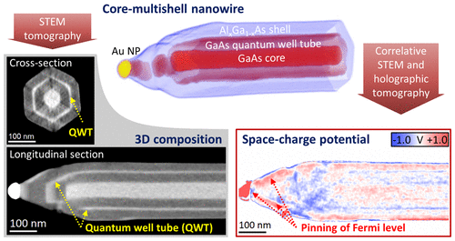
The nondestructive characterization of nanoscale devices, such as those based on semiconductor nanowires, in terms of functional potentials is crucial for correlating device properties with their morphological/materials features, as well as for precisely tuning and optimizing their growth process. Electron holographic tomography (EHT) has been used in the past to reconstruct the total potential distribution in three-dimension but hitherto lacked a quantitative approach to separate potential variations due to chemical composition changes (mean inner potential, MIP) and space charges. In this Letter, we combine and correlate EHT and high-angle annular dark-field scanning transmission electron microscopy (HAADF-STEM) tomography on an individual ⟨111⟩ oriented GaAs-AlGaAs core-multishell nanowire (NW). We obtain excellent agreement between both methods in terms of the determined Al concentration within the AlGaAs shell, as well as thickness variations of the few nanometer thin GaAs shell acting as quantum well tube. Subtracting the MIP determined from the STEM tomogram, enables us to observe functional potentials at the NW surfaces and at the Au-NW interface, both ascribed to surface/interface pinning of the semiconductor Fermi level.
中文翻译:

III-V核-多壳纳米线的三维组成和电势映射的相关STEM和全息层析成像。
就功能电位而言,纳米级器件(例如基于半导体纳米线的器件)的非破坏性表征对于将器件性能与其形态/材料特征相关联以及精确调整和优化其生长过程至关重要。过去曾使用电子全息断层扫描(EHT)来重建三维的总电势分布,但是迄今为止,由于化学成分的变化(平均内部电势,MIP)和空间电荷,目前尚缺乏定量方法来分离电势变化。在这封信中,我们结合了EHT和高角度环形暗场扫描透射电子显微镜(HAADF-STEM)层析成像,并将其关联在单个⟨111取向的GaAs-AlGaAs核-多壳纳米线(NW)上。我们在确定的AlGaAs壳内Al浓度以及少数用作量子阱管的纳米GaAs薄壳的厚度变化方面,在两种方法之间都取得了极好的一致性。减去从STEM断层图中确定的MIP,使我们能够观察到NW表面和Au-NW界面处的功能电位,两者均归因于半导体费米能级的表面/界面固定。
更新日期:2018-07-13
中文翻译:
III-V核-多壳纳米线的三维组成和电势映射的相关STEM和全息层析成像。
就功能电位而言,纳米级器件(例如基于半导体纳米线的器件)的非破坏性表征对于将器件性能与其形态/材料特征相关联以及精确调整和优化其生长过程至关重要。过去曾使用电子全息断层扫描(EHT)来重建三维的总电势分布,但是迄今为止,由于化学成分的变化(平均内部电势,MIP)和空间电荷,目前尚缺乏定量方法来分离电势变化。在这封信中,我们结合了EHT和高角度环形暗场扫描透射电子显微镜(HAADF-STEM)层析成像,并将其关联在单个⟨111取向的GaAs-AlGaAs核-多壳纳米线(NW)上。我们在确定的AlGaAs壳内Al浓度以及少数用作量子阱管的纳米GaAs薄壳的厚度变化方面,在两种方法之间都取得了极好的一致性。减去从STEM断层图中确定的MIP,使我们能够观察到NW表面和Au-NW界面处的功能电位,两者均归因于半导体费米能级的表面/界面固定。


 京公网安备 11010802027423号