Organic Electronics ( IF 3.2 ) Pub Date : 2018-06-30 , DOI: 10.1016/j.orgel.2018.06.053 Ute Zschieschang , James W. Borchert , Michael Geiger , Florian Letzkus , Joachim N. Burghartz , Hagen Klauk
|
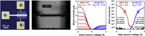
For some of the more demanding applications envisioned for organic transistors, lateral device dimensions of less than 1 μm may be necessary or should at least be explored in order to evaluate the scalability of organic transistors. Using stencil lithography based on high-resolution silicon stencil masks and employing two small-molecule organic semiconductors with good long-term air stability, we have fabricated organic p-channel and n-channel transistors with a channel length of 0.3 μm. Owing to the small channel length, the transistors have large channel-width-normalized transconductances (1.5 S/m for the p-channel and 0.2 S/m for the n-channel transistors). In addition, the transistors have steep subthreshold slopes (80 and 200 mV/decade) and large on/off current ratios (106).
中文翻译:
通道长度为300 nm的有机薄膜晶体管的模板光刻
对于针对有机晶体管设想的一些更苛刻的应用,可能需要或应探索小于1μm的横向器件尺寸,以便评估有机晶体管的可扩展性。使用基于高分辨率硅模板掩模的模板光刻技术,并使用两种具有良好长期空气稳定性的小分子有机半导体,我们制作了沟道长度为0.3μm的有机p沟道和n沟道晶体管。由于沟道长度小,这些晶体管具有大的沟道宽度归一化跨导(p沟道为1.5 S / m,n沟道晶体管为0.2 S / m)。另外,晶体管具有陡峭的亚阈值斜率(80和200 mV /十倍)和大的开/关电流比(10 6)。


 京公网安备 11010802027423号