Nano Energy ( IF 17.6 ) Pub Date : 2018-06-26 , DOI: 10.1016/j.nanoen.2018.06.079 Jian Lv , Meiling Xu , Shiru Lin , Xuecheng Shao , Xinyu Zhang , Yanhui Liu , Yanchao Wang , Zhongfang Chen , Yanming Ma
|
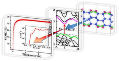
Crystalline silicon is dominating the current solar cell market due to the significant efficiency improvement and cost reduction in last decades. However, its indirect band gap nature leads to inefficient visible-light absorption, which seriously impedes further performance enhancement in silicon-based photovoltaic devices. Thus, it is highly desirable to develop direct band gap silicon materials. Herein, by means of ab initio swarm-intelligence structure-searching method, we predicted a quasi-direct gap semiconducting tri-layer silicene structure consisting of alternating arrays of six-membered Si rings, which can be converted into a direct gap semiconductor of 0.86 eV by applying a low tensile strain (~ 2.5%). Our calculations revealed that the photovoltaic efficiency of the tri-layer silicene reaches 29% at 1.0 µm, which is comparable to that of bulk GaAs with the highest conversion efficiency among thin-film solar cell absorbers.
中文翻译:
具有29%光伏效率的直接间隙半导体三层硅
由于近几十年来效率的显着提高和成本的降低,晶体硅在当前的太阳能电池市场中占据着主导地位。然而,其间接的带隙性质导致无效的可见光吸收,这严重阻碍了基于硅的光伏器件中进一步的性能增强。因此,非常需要开发直接带隙硅材料。在本文中,通过从头算起的群体智能结构搜索方法,我们预测了由六元硅环的交替阵列组成的准直接间隙半导体三层硅结构,可以将其转换为0.86的直接间隙半导体通过施加低拉伸应变(〜2.5%)来实现eV。我们的计算表明,三层硅的光伏效率在1.0 µm时达到29%,


 京公网安备 11010802027423号