当前位置:
X-MOL 学术
›
Adv. Funct. Mater.
›
论文详情
Our official English website, www.x-mol.net, welcomes your feedback! (Note: you will need to create a separate account there.)
Asymmetric Schottky Contacts in Bilayer MoS2 Field Effect Transistors
Advanced Functional Materials ( IF 19.0 ) Pub Date : 2018-05-21 , DOI: 10.1002/adfm.201800657 Antonio Di Bartolomeo 1 , Alessandro Grillo 1 , Francesca Urban 1 , Laura Iemmo 1 , Filippo Giubileo 2 , Giuseppe Luongo 1 , Giampiero Amato 3 , Luca Croin 3 , Linfeng Sun 4 , Shi-Jun Liang 5, 6 , Lay Kee Ang 5
Advanced Functional Materials ( IF 19.0 ) Pub Date : 2018-05-21 , DOI: 10.1002/adfm.201800657 Antonio Di Bartolomeo 1 , Alessandro Grillo 1 , Francesca Urban 1 , Laura Iemmo 1 , Filippo Giubileo 2 , Giuseppe Luongo 1 , Giampiero Amato 3 , Luca Croin 3 , Linfeng Sun 4 , Shi-Jun Liang 5, 6 , Lay Kee Ang 5
Affiliation
|
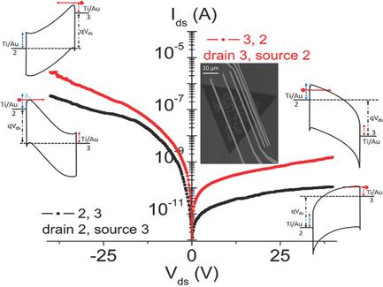
The high‐bias electrical characteristics of back‐gated field‐effect transistors with chemical vapor deposition synthesized bilayer MoS2 channel and Ti Schottky contacts are discussed. It is found that oxidized Ti contacts on MoS2 form rectifying junctions with ≈0.3 to 0.5 eV Schottky barrier height. To explain the rectifying output characteristics of the transistors, a model is proposed based on two slightly asymmetric back‐to‐back Schottky barriers, where the highest current arises from image force barrier lowering at the electrically forced junction, while the reverse current is due to Schottky‐barrier‐limited injection at the grounded junction. The device achieves a photoresponsivity greater than 2.5 A W−1 under 5 mW cm−2 white‐LED light. By comparing two‐ and four‐probe measurements, it is demonstrated that the hysteresis and persistent photoconductivity exhibited by the transistor are peculiarities of the MoS2 channel rather than effects of the Ti/MoS2 interface.
中文翻译:

双层MoS2场效应晶体管中的不对称肖特基接触
讨论了具有化学气相沉积合成双层MoS 2沟道和Ti肖特基接触的背栅场效应晶体管的高偏置电特性。发现在MoS 2上氧化的Ti触点形成具有约0.3至0.5 eV肖特基势垒高度的整流结。为了解释晶体管的整流输出特性,基于两个略微不对称的背对背肖特基势垒,提出了一个模型,其中最大电流来自在电动结处的镜像力势垒降低,而反向电流是由于接地结点处的肖特基势垒限制注入。该器件在5 mW cm -2下实现了大于2.5 AW -1的光响应白色LED灯。通过比较两个和四个探针的测量结果,可以证明晶体管表现出的磁滞和持久光电导是MoS 2通道的特性,而不是Ti / MoS 2界面的影响。
更新日期:2018-05-21
中文翻译:
双层MoS2场效应晶体管中的不对称肖特基接触
讨论了具有化学气相沉积合成双层MoS 2沟道和Ti肖特基接触的背栅场效应晶体管的高偏置电特性。发现在MoS 2上氧化的Ti触点形成具有约0.3至0.5 eV肖特基势垒高度的整流结。为了解释晶体管的整流输出特性,基于两个略微不对称的背对背肖特基势垒,提出了一个模型,其中最大电流来自在电动结处的镜像力势垒降低,而反向电流是由于接地结点处的肖特基势垒限制注入。该器件在5 mW cm -2下实现了大于2.5 AW -1的光响应白色LED灯。通过比较两个和四个探针的测量结果,可以证明晶体管表现出的磁滞和持久光电导是MoS 2通道的特性,而不是Ti / MoS 2界面的影响。


 京公网安备 11010802027423号