当前位置:
X-MOL 学术
›
J. Phys. Chem. C
›
论文详情
Our official English website, www.x-mol.net, welcomes your feedback! (Note: you will need to create a separate account there.)
Atomic-Scale Electronic Characterization of Defects in Silicon Carbide Nanowires by Electron Energy-Loss Spectroscopy
The Journal of Physical Chemistry C ( IF 3.7 ) Pub Date : 2018-05-10 00:00:00 , DOI: 10.1021/acs.jpcc.8b01661 Lunet E. Luna 1 , David Gardner 1 , Velimir Radmilovic 2, 3 , Roya Maboudian 1 , Carlo Carraro 1
The Journal of Physical Chemistry C ( IF 3.7 ) Pub Date : 2018-05-10 00:00:00 , DOI: 10.1021/acs.jpcc.8b01661 Lunet E. Luna 1 , David Gardner 1 , Velimir Radmilovic 2, 3 , Roya Maboudian 1 , Carlo Carraro 1
Affiliation
|
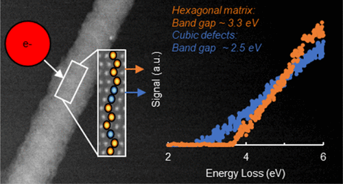
The atomic-level resolution of scanning transmission electron microscopy (TEM) is used for structural characterization of nanomaterials, but the resolution afforded by TEM also enables electronic characterization of defects in these materials through electron energy-loss spectroscopy (EELS). Here, the power of EELS is harnessed to characterize the local band gap of inclusion defects in hexagonal silicon carbide nanowires with a high density of stacking faults. The band gaps we extract from the EELS data align within 0.1 eV of expected values for hexagonal silicon carbide and stacking faults within hexagonal silicon carbide. These experiments show that individual cubic phase inclusions in hexagonal silicon carbide significantly alter the local electronic structure, in particular, the band gap, in contrast to the polarizability tensor that retains the characteristic signature of the global hexagonal crystal structure.
中文翻译:

电子能损谱的碳化硅纳米线缺陷的原子尺度电子表征
扫描透射电子显微镜(TEM)的原子级分辨率用于纳米材料的结构表征,但是TEM提供的分辨率还可以通过电子能量损失谱(EELS)对这些材料中的缺陷进行电子表征。在这里,利用EELS的能力来表征具有高堆积缺陷密度的六角形碳化硅纳米线中夹杂缺陷的局部带隙。我们从EELS数据中提取的带隙在六角形碳化硅和六角形碳化硅内的堆垛层错的预期值的0.1 eV范围内对齐。这些实验表明,六角形碳化硅中的各个立方相夹杂物会显着改变局部电子结构,特别是带隙,
更新日期:2018-05-10
中文翻译:
电子能损谱的碳化硅纳米线缺陷的原子尺度电子表征
扫描透射电子显微镜(TEM)的原子级分辨率用于纳米材料的结构表征,但是TEM提供的分辨率还可以通过电子能量损失谱(EELS)对这些材料中的缺陷进行电子表征。在这里,利用EELS的能力来表征具有高堆积缺陷密度的六角形碳化硅纳米线中夹杂缺陷的局部带隙。我们从EELS数据中提取的带隙在六角形碳化硅和六角形碳化硅内的堆垛层错的预期值的0.1 eV范围内对齐。这些实验表明,六角形碳化硅中的各个立方相夹杂物会显着改变局部电子结构,特别是带隙,


 京公网安备 11010802027423号