当前位置:
X-MOL 学术
›
Nano Lett.
›
论文详情
Our official English website, www.x-mol.net, welcomes your feedback! (Note: you will need to create a separate account there.)
Nanopatterned High-Frequency Supporting Structures Stably Eliminate Substrate Effects Imposed on Two-Dimensional Semiconductors
Nano Letters ( IF 10.8 ) Pub Date : 2018-04-03 00:00:00 , DOI: 10.1021/acs.nanolett.8b00084 Soonmin Yim 1 , Hyeuk Jin Han 1 , Jaebeom Jeon 1 , Kiung Jeon 1 , Dong Min Sim 1 , Yeon Sik Jung 1
Nano Letters ( IF 10.8 ) Pub Date : 2018-04-03 00:00:00 , DOI: 10.1021/acs.nanolett.8b00084 Soonmin Yim 1 , Hyeuk Jin Han 1 , Jaebeom Jeon 1 , Kiung Jeon 1 , Dong Min Sim 1 , Yeon Sik Jung 1
Affiliation
|
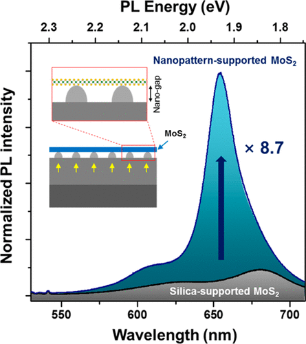
Despite the outstanding physical and chemical properties of two-dimensional (2D) materials, due to their extremely thin nature, eliminating detrimental substrate effects such as serious degradation of charge-carrier mobility or light-emission yield remains a major challenge. However, previous approaches have suffered from limitations such as structural instability or the need of costly and high-temperature deposition processes. Herein, we propose a new strategy based on the insertion of high-density topographic nanopatterns as a nanogap-containing supporter between 2D materials and substrate to minimize their contact and to block the substrate-induced undesirable effects. We show that well-controlled high-frequency SiOx nanopillar structures derived from the self-assembly of Si-containing block copolymer securely prevent the collapse or deformation of transferred MoS2 and guarantee excellent mechanical stability. The nanogap supporters formed below monolayer MoS2 lead to dramatic enhancement of the photoluminescence emission intensity (8.7-fold), field-effect mobility (2.0-fold, with a maximum of 4.3-fold), and photoresponsivity (12.1-fold) compared to the sample on flat SiO2. Similar favorable effects observed for graphene strongly suggest that this simple but powerful nanogap-supporting method can be extensively applicable to a variety of low-dimensional materials and contribute to improved device performance.
中文翻译:

纳米图案化的高频支撑结构稳定地消除了施加在二维半导体上的基板效应
尽管二维(2D)材料具有出色的物理和化学特性,但由于其极薄的性质,要消除有害的衬底效应(例如电荷载流子迁移率或发光产率的严重下降)仍然是一个主要挑战。然而,先前的方法受到诸如结构不稳定性或需要昂贵的高温沉积工艺的限制。本文中,我们提出了一种新策略,该策略基于在2D材料和基板之间插入高密度形貌纳米图形作为含纳米间隙的支撑物,以最大程度地减少它们之间的接触并阻止基板引起的不良影响。我们表明,控制良好的高频SiO x源自含硅嵌段共聚物自组装的纳米柱结构可安全地防止转移的MoS 2塌陷或变形,并确保出色的机械稳定性。与单层MoS 2下方形成的纳米间隙支持物相比,光致发光发射强度(8.7倍),场效应迁移率(2.0倍,最大4.3倍)和光响应性(12.1倍)显着提高。样品在平坦的SiO 2上。对于石墨烯观察到的类似有利效果有力地表明,这种简单但功能强大的纳米间隙支撑方法可广泛应用于各种低维材料,并有助于改善器件性能。
更新日期:2018-04-03
中文翻译:
纳米图案化的高频支撑结构稳定地消除了施加在二维半导体上的基板效应
尽管二维(2D)材料具有出色的物理和化学特性,但由于其极薄的性质,要消除有害的衬底效应(例如电荷载流子迁移率或发光产率的严重下降)仍然是一个主要挑战。然而,先前的方法受到诸如结构不稳定性或需要昂贵的高温沉积工艺的限制。本文中,我们提出了一种新策略,该策略基于在2D材料和基板之间插入高密度形貌纳米图形作为含纳米间隙的支撑物,以最大程度地减少它们之间的接触并阻止基板引起的不良影响。我们表明,控制良好的高频SiO x源自含硅嵌段共聚物自组装的纳米柱结构可安全地防止转移的MoS 2塌陷或变形,并确保出色的机械稳定性。与单层MoS 2下方形成的纳米间隙支持物相比,光致发光发射强度(8.7倍),场效应迁移率(2.0倍,最大4.3倍)和光响应性(12.1倍)显着提高。样品在平坦的SiO 2上。对于石墨烯观察到的类似有利效果有力地表明,这种简单但功能强大的纳米间隙支撑方法可广泛应用于各种低维材料,并有助于改善器件性能。


 京公网安备 11010802027423号