Our official English website, www.x-mol.net, welcomes your feedback! (Note: you will need to create a separate account there.)
Graphene as an Imaging Platform of Charged Molecules
ACS Omega ( IF 4.1 ) Pub Date : 2018-03-15 00:00:00 , DOI: 10.1021/acsomega.7b02008 Shota Ushiba 1 , Takao Ono 2 , Yasushi Kanai 2 , Koichi Inoue 2 , Masahiko Kimura 1 , Kazuhiko Matsumoto 2
ACS Omega ( IF 4.1 ) Pub Date : 2018-03-15 00:00:00 , DOI: 10.1021/acsomega.7b02008 Shota Ushiba 1 , Takao Ono 2 , Yasushi Kanai 2 , Koichi Inoue 2 , Masahiko Kimura 1 , Kazuhiko Matsumoto 2
Affiliation
|
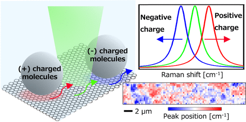
Graphene, a single atom layer of carbon atoms, provides a two-dimensional platform with an extremely high sensitivity to charges due to its unique band structure and high surface-to-volume ratio. Graphene field-effect transistor (G-FET) biosensors have, indeed, demonstrated a detection limit of subnanomolar or even subpicomolar. However, in G-FET, signal is averaged throughout the whole channel, so there remains a need to visualize the spatial distribution of target molecules on a single G-FET, to provide further insight into target molecules and/or biological functions. Here, we made use of graphene as an imaging platform of charged molecules via Raman microscopy. Positively (or negatively) charged microbeads with a diameter of 1 μm were dispersed in a buffer solution and were attached on graphene. We found out that Raman peaks of graphene, where positively (or negatively) charged beads contacted, were up-shifted (or down-shifted) significantly, indicating that the carrier density in the graphene was locally modulated by the charged beads and the charge state of the beads was represented by the peak-shift direction. From the peak shift, the change in the carrier density was calculated to be +1.4 × 1012 cm–2 (or −1.0 × 1012 cm–2). By taking Raman peak-shift images, we visualized distribution of charged molecules on graphene with a spatial resolution below 1 μm. The technique described here overcomes the limitation of spatial resolution of G-FET and provides a new route to graphene-based chemical and biosensors.
中文翻译:

石墨烯作为带电分子的成像平台
石墨烯是碳原子的单原子层,由于其独特的能带结构和高的体积比,提供了一个对电荷具有极高灵敏度的二维平台。石墨烯场效应晶体管(G-FET)生物传感器确实已经证明了亚纳摩尔甚至亚皮摩尔的检测极限。然而,在G-FET中,信号是在整个通道中平均的,因此仍然需要可视化单个G-FET上目标分子的空间分布,以进一步了解目标分子和/或生物学功能。在这里,我们通过拉曼显微镜将石墨烯用作带电分子的成像平台。将直径为1μm的带正电(或带负电)的微珠分散在缓冲溶液中,并附着在石墨烯上。我们发现石墨烯的拉曼峰 接触带正电(或带负电)的珠子的位置显着上移(或下移),表明石墨烯中的载流子密度受到带电珠子的局部调节,并且该珠子的电荷状态由峰-转移方向。根据峰位移,计算出载流子密度的变化为+1.4×1012 cm –2(或−1.0×10 12 cm –2)。通过拍摄拉曼峰移图像,我们可以看到带电分子在石墨烯上的分布,其空间分辨率低于1μm。此处描述的技术克服了G-FET的空间分辨率的局限性,并为基于石墨烯的化学和生物传感器提供了一条新途径。
更新日期:2018-03-15
中文翻译:
石墨烯作为带电分子的成像平台
石墨烯是碳原子的单原子层,由于其独特的能带结构和高的体积比,提供了一个对电荷具有极高灵敏度的二维平台。石墨烯场效应晶体管(G-FET)生物传感器确实已经证明了亚纳摩尔甚至亚皮摩尔的检测极限。然而,在G-FET中,信号是在整个通道中平均的,因此仍然需要可视化单个G-FET上目标分子的空间分布,以进一步了解目标分子和/或生物学功能。在这里,我们通过拉曼显微镜将石墨烯用作带电分子的成像平台。将直径为1μm的带正电(或带负电)的微珠分散在缓冲溶液中,并附着在石墨烯上。我们发现石墨烯的拉曼峰 接触带正电(或带负电)的珠子的位置显着上移(或下移),表明石墨烯中的载流子密度受到带电珠子的局部调节,并且该珠子的电荷状态由峰-转移方向。根据峰位移,计算出载流子密度的变化为+1.4×1012 cm –2(或−1.0×10 12 cm –2)。通过拍摄拉曼峰移图像,我们可以看到带电分子在石墨烯上的分布,其空间分辨率低于1μm。此处描述的技术克服了G-FET的空间分辨率的局限性,并为基于石墨烯的化学和生物传感器提供了一条新途径。


 京公网安备 11010802027423号