当前位置:
X-MOL 学术
›
Adv. Electron. Mater.
›
论文详情
Our official English website, www.x-mol.net, welcomes your feedback! (Note: you will need to create a separate account there.)
Controlled Growth of Bilayer‐MoS2 Films and MoS2‐Based Field‐Effect Transistor (FET) Performance Optimization
Advanced Electronic Materials ( IF 6.2 ) Pub Date : 2018-03-14 , DOI: 10.1002/aelm.201700524 Mingxu Fang 1 , Fang Wang 1 , Yemei Han 1 , Yulin Feng 1 , Tianling Ren 2 , Yue Li 1 , Dengxuan Tang 1 , Zhitang Song 3 , Kailiang Zhang 1
Advanced Electronic Materials ( IF 6.2 ) Pub Date : 2018-03-14 , DOI: 10.1002/aelm.201700524 Mingxu Fang 1 , Fang Wang 1 , Yemei Han 1 , Yulin Feng 1 , Tianling Ren 2 , Yue Li 1 , Dengxuan Tang 1 , Zhitang Song 3 , Kailiang Zhang 1
Affiliation
|
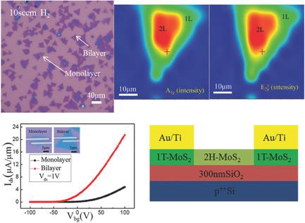
The effect of hydrogen flow on MoS2 film synthesis via chemical vapor deposition is studied systematically. Large‐sized monolayer‐ and bilayer‐MoS2 triangles can be synthesized controllably at given temperatures. Optical microscopy, Raman spectroscopy, photoluminescence spectroscopy, and atomic force microscopy are used to characterize the number of layers, purity, and uniformity of the MoS2 triangle films. Moreover, the back‐gated field‐effect transistors (FETs) based on the monolayer‐ and bilayer‐MoS2 channels are fabricated using traditional micro‐nanoprocessing technology. Electrical behaviors are investigated and the bilayer‐MoS2 FETs show preferable performance with high mobility (≈21 cm2 V−1 s−1), on‐current (≈22 µA µm−1), and a small degradation in the on/off ratio (1.1 × 10⁷). Finally, the semiconductive phase MoS2 (2H‐MoS2) is transformed to a metallic phase (1T‐MoS2) to reduce the resistance in metal‐MoS2 contact. The FET device with 1T‐MoS2 contact enhances mobility (≈45 cm2 V−1 s−1) and on‐current (≈50 µA µm−1) compared with the 2H‐MoS2 FETs. This work sheds light on the synthesis of variable‐layer MoS2 films and paves the way for further development regarding MoS2 film‐based devices.
中文翻译:

双层MoS2薄膜的受控生长和基于MoS2的场效应晶体管(FET)性能优化
系统地研究了氢流对化学气相沉积合成MoS 2薄膜的影响。可以在给定温度下可控地合成大型单层和双层MoS 2三角形。光学显微镜,拉曼光谱,光致发光光谱和原子力显微镜用于表征MoS 2三角形薄膜的层数,纯度和均匀性。此外,基于单层和双层MoS 2通道的背栅场效应晶体管(FET)是使用传统的微纳米加工技术制造的。对电气行为进行了研究,双层MoS 2 FET在高迁移率(≈21cm 2V -1 s -1),导通电流(≈22µA µm -1)和开/关比的小幅度下降(1.1×10 7)。最后,将半导体相MoS 2(2H-MoS 2)转变为金属相(1T-MoS 2),以降低金属-MoS 2接触中的电阻。与2H-MoS 2 FET相比,具有1T-MoS 2触点的FET器件可提高迁移率(≈45cm 2 V -1 s -1)和导通电流(≈50µA µm -1)。这项工作为可变层MoS 2的合成提供了启示拍摄并为基于MoS 2胶片的设备的进一步开发铺平了道路。
更新日期:2018-03-14
中文翻译:
双层MoS2薄膜的受控生长和基于MoS2的场效应晶体管(FET)性能优化
系统地研究了氢流对化学气相沉积合成MoS 2薄膜的影响。可以在给定温度下可控地合成大型单层和双层MoS 2三角形。光学显微镜,拉曼光谱,光致发光光谱和原子力显微镜用于表征MoS 2三角形薄膜的层数,纯度和均匀性。此外,基于单层和双层MoS 2通道的背栅场效应晶体管(FET)是使用传统的微纳米加工技术制造的。对电气行为进行了研究,双层MoS 2 FET在高迁移率(≈21cm 2V -1 s -1),导通电流(≈22µA µm -1)和开/关比的小幅度下降(1.1×10 7)。最后,将半导体相MoS 2(2H-MoS 2)转变为金属相(1T-MoS 2),以降低金属-MoS 2接触中的电阻。与2H-MoS 2 FET相比,具有1T-MoS 2触点的FET器件可提高迁移率(≈45cm 2 V -1 s -1)和导通电流(≈50µA µm -1)。这项工作为可变层MoS 2的合成提供了启示拍摄并为基于MoS 2胶片的设备的进一步开发铺平了道路。


 京公网安备 11010802027423号