当前位置:
X-MOL 学术
›
J. Phys. Chem. Lett.
›
论文详情
Our official English website, www.x-mol.net, welcomes your feedback! (Note: you will need to create a separate account there.)
Spin-Coated Crystalline Molecular Monolayers for Performance Enhancement in Organic Field-Effect Transistors
The Journal of Physical Chemistry Letters ( IF 5.7 ) Pub Date : 2018-03-01 00:00:00 , DOI: 10.1021/acs.jpclett.8b00352 Qijing Wang 1, 2 , Emilio J. Juarez-Perez 2 , Sai Jiang 1 , Longbin Qiu 2 , Luis K. Ono 2 , Toshio Sasaki 3 , Xinran Wang 1 , Yi Shi 1 , Youdou Zheng 1 , Yabing Qi 2 , Yun Li 1
The Journal of Physical Chemistry Letters ( IF 5.7 ) Pub Date : 2018-03-01 00:00:00 , DOI: 10.1021/acs.jpclett.8b00352 Qijing Wang 1, 2 , Emilio J. Juarez-Perez 2 , Sai Jiang 1 , Longbin Qiu 2 , Luis K. Ono 2 , Toshio Sasaki 3 , Xinran Wang 1 , Yi Shi 1 , Youdou Zheng 1 , Yabing Qi 2 , Yun Li 1
Affiliation
|
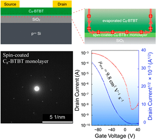
In organic field-effect transistors, the first few molecular layers at the semiconductor/dielectric interface are regarded as the active channel for charge transport; thus, great efforts have been devoted to the modification and optimization of molecular packing at such interfaces. Here, we report organic monolayers with large-area uniformity and high crystallinity deposited by an antisolvent-assisted spin-coating method acting as the templating layers between the dielectric and thermally evaporated semiconducting layers. The predeposited crystalline monolayers significantly enhance the film crystallinity of upper layers and the overall performance of transistors using these hybrid-deposited semiconducting films, showing a high carrier mobility up to 11.3 cm2 V–1 s–1. Additionally, patterned transistor arrays composed of the templating monolayers are fabricated, yielding an average mobility of 7.7 cm2 V–1 s–1. This work demonstrates a promising method for fabricating low-cost, high-performance, and large-area organic electronics.
中文翻译:

旋转涂覆的晶体分子单分子层,用于增强有机场效应晶体管的性能
在有机场效应晶体管中,半导体/电介质界面上的前几个分子层被视为电荷传输的有源通道。因此,在这种界面上的分子堆积的修饰和最优化方面已付出了巨大的努力。在这里,我们报道了通过反溶剂辅助旋涂法沉积的具有大面积均匀性和高结晶度的有机单分子层,它们用作介电层和热蒸发半导体层之间的模板层。预沉积的晶体单层显着提高了上层的膜的结晶度,并提高了使用这些混合沉积的半导体膜的晶体管的整体性能,显示出高达11.3 cm 2 V –1 s –1的高载流子迁移率。此外,还制作了由模板单层组成的图案化晶体管阵列,平均迁移率为7.7 cm 2 V –1 s –1。这项工作展示了一种制造低成本,高性能和大面积有机电子产品的有前途的方法。
更新日期:2018-03-01
中文翻译:
旋转涂覆的晶体分子单分子层,用于增强有机场效应晶体管的性能
在有机场效应晶体管中,半导体/电介质界面上的前几个分子层被视为电荷传输的有源通道。因此,在这种界面上的分子堆积的修饰和最优化方面已付出了巨大的努力。在这里,我们报道了通过反溶剂辅助旋涂法沉积的具有大面积均匀性和高结晶度的有机单分子层,它们用作介电层和热蒸发半导体层之间的模板层。预沉积的晶体单层显着提高了上层的膜的结晶度,并提高了使用这些混合沉积的半导体膜的晶体管的整体性能,显示出高达11.3 cm 2 V –1 s –1的高载流子迁移率。此外,还制作了由模板单层组成的图案化晶体管阵列,平均迁移率为7.7 cm 2 V –1 s –1。这项工作展示了一种制造低成本,高性能和大面积有机电子产品的有前途的方法。


 京公网安备 11010802027423号