Our official English website, www.x-mol.net, welcomes your feedback! (Note: you will need to create a separate account there.)
Hole Transport in Exfoliated Monolayer MoS2
ACS Nano ( IF 17.1 ) Pub Date : 2018-02-26 00:00:00 , DOI: 10.1021/acsnano.7b08831 Evgeniy Ponomarev , Árpád Pásztor , Adrien Waelchli , Alessandro Scarfato , Nicolas Ubrig , Christoph Renner , Alberto F. Morpurgo
ACS Nano ( IF 17.1 ) Pub Date : 2018-02-26 00:00:00 , DOI: 10.1021/acsnano.7b08831 Evgeniy Ponomarev , Árpád Pásztor , Adrien Waelchli , Alessandro Scarfato , Nicolas Ubrig , Christoph Renner , Alberto F. Morpurgo
|
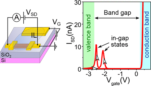
Ideal monolayers of common semiconducting transition-metal dichalcogenides (TMDCs) such as MoS2, WS2, MoSe2, and WSe2 possess many similar electronic properties. As it is the case for all semiconductors, however, the physical response of these systems is strongly determined by defects in a way specific to each individual compound. Here we investigate the ability of exfoliated monolayers of these TMDCs to support high-quality, well-balanced ambipolar conduction, which has been demonstrated for WS2, MoSe2, and WSe2, but not for MoS2. Using ionic-liquid gated transistors, we show that, contrary to WS2, MoSe2, and WSe2, hole transport in exfoliated MoS2 monolayers is systematically anomalous, exhibiting a maximum in conductivity at negative gate voltage (VG) followed by a suppression of up to 100 times upon further increasing VG. To understand the origin of this difference, we have performed a series of experiments including the comparison of hole transport in MoS2 monolayers and thicker multilayers, in exfoliated and CVD-grown monolayers, as well as gate-dependent optical measurements (Raman and photoluminescence) and scanning tunneling imaging and spectroscopy. In agreement with existing ab initio calculations, the results of all these experiments are consistently explained in terms of defects associated with chalcogen vacancies that only in MoS2 monolayers, but not in thicker MoS2 multilayers nor in monolayers of the other common semiconducting TMDCs, create in-gap states near the top of the valence band that act as strong hole traps. Our results demonstrate the importance of studying systematically how defects determine the properties of 2D semiconducting materials and of developing methods to control them.
中文翻译:

剥离单层MoS 2中的空穴传输
常见的半导体过渡金属二硫化碳(TMDC)的理想单层,例如MoS 2,WS 2,MoSe 2和WSe 2具有许多相似的电子特性。但是,就像所有半导体一样,这些系统的物理响应在很大程度上取决于缺陷,具体取决于每种化合物的特定方式。在这里,我们研究了这些TMDC的剥落单层支持高质量,平衡双极性传导的能力,这已针对WS 2,MoSe 2和WSe 2进行了证明,但对于MoS 2却未得到证明。使用离子液体门控晶体管,我们证明与WS 2相反,MoSe如图2和WSe 2所示,剥落的MoS 2单层中的空穴传输系统地异常,在负栅极电压(V G)处显示出最大的电导率,随后在进一步增加V G时抑制多达100倍。为了了解这种差异的起因,我们进行了一系列实验,包括比较MoS 2单层和较厚的多层,在剥离的和CVD生长的单层中的空穴传输,以及与门相关的光学测量(拉曼光谱和光致发光)以及扫描隧道成像和光谱学。与现有的从头算起达成协议计算中,所有这些实验的结果均根据与硫属元素空位有关的缺陷得到了一致的解释,该缺陷仅在MoS 2单层中,而在较厚的MoS 2多层中或在其他常见的半导体TMDC的单层中却不形成,从而在硅的附近形成带隙状态。在价带的顶部,用作强空穴陷阱。我们的结果表明,必须系统地研究缺陷如何确定2D半导体材料的特性以及控制它们的开发方法的重要性。
更新日期:2018-02-26
中文翻译:
剥离单层MoS 2中的空穴传输
常见的半导体过渡金属二硫化碳(TMDC)的理想单层,例如MoS 2,WS 2,MoSe 2和WSe 2具有许多相似的电子特性。但是,就像所有半导体一样,这些系统的物理响应在很大程度上取决于缺陷,具体取决于每种化合物的特定方式。在这里,我们研究了这些TMDC的剥落单层支持高质量,平衡双极性传导的能力,这已针对WS 2,MoSe 2和WSe 2进行了证明,但对于MoS 2却未得到证明。使用离子液体门控晶体管,我们证明与WS 2相反,MoSe如图2和WSe 2所示,剥落的MoS 2单层中的空穴传输系统地异常,在负栅极电压(V G)处显示出最大的电导率,随后在进一步增加V G时抑制多达100倍。为了了解这种差异的起因,我们进行了一系列实验,包括比较MoS 2单层和较厚的多层,在剥离的和CVD生长的单层中的空穴传输,以及与门相关的光学测量(拉曼光谱和光致发光)以及扫描隧道成像和光谱学。与现有的从头算起达成协议计算中,所有这些实验的结果均根据与硫属元素空位有关的缺陷得到了一致的解释,该缺陷仅在MoS 2单层中,而在较厚的MoS 2多层中或在其他常见的半导体TMDC的单层中却不形成,从而在硅的附近形成带隙状态。在价带的顶部,用作强空穴陷阱。我们的结果表明,必须系统地研究缺陷如何确定2D半导体材料的特性以及控制它们的开发方法的重要性。


 京公网安备 11010802027423号