当前位置:
X-MOL 学术
›
Adv. Funct. Mater.
›
论文详情
Our official English website, www.x-mol.net, welcomes your feedback! (Note: you will need to create a separate account there.)
Tuning the Electronic and Photonic Properties of Monolayer MoS2 via In Situ Rhenium Substitutional Doping
Advanced Functional Materials ( IF 19.0 ) Pub Date : 2018-02-16 , DOI: 10.1002/adfm.201706950 Kehao Zhang 1, 2 , Brian M. Bersch 1 , Jaydeep Joshi 3 , Rafik Addou 4 , Christopher R. Cormier 4 , Chenxi Zhang 4 , Ke Xu 5 , Natalie C. Briggs 1 , Ke Wang 6 , Shruti Subramanian 1 , Kyeongjae Cho 4 , Susan Fullerton-Shirey 5, 7 , Robert M. Wallace 4 , Patrick M. Vora 3 , Joshua A. Robinson 1, 2
Advanced Functional Materials ( IF 19.0 ) Pub Date : 2018-02-16 , DOI: 10.1002/adfm.201706950 Kehao Zhang 1, 2 , Brian M. Bersch 1 , Jaydeep Joshi 3 , Rafik Addou 4 , Christopher R. Cormier 4 , Chenxi Zhang 4 , Ke Xu 5 , Natalie C. Briggs 1 , Ke Wang 6 , Shruti Subramanian 1 , Kyeongjae Cho 4 , Susan Fullerton-Shirey 5, 7 , Robert M. Wallace 4 , Patrick M. Vora 3 , Joshua A. Robinson 1, 2
Affiliation
|
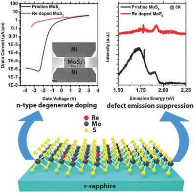
Doping is a fundamental requirement for tuning and improving the properties of conventional semiconductors. Recent doping studies including niobium (Nb) doping of molybdenum disulfide (MoS2) and tungsten (W) doping of molybdenum diselenide (MoSe2) have suggested that substitutional doping may provide an efficient route to tune the doping type and suppress deep trap levels of 2D materials. To date, the impact of the doping on the structural, electronic, and photonic properties of in situ‐doped monolayers remains unanswered due to challenges including strong film substrate charge transfer, and difficulty achieving doping concentrations greater than 0.3 at%. Here, in situ rhenium (Re) doping of synthetic monolayer MoS2 with ≈1 at% Re is demonstrated. To limit substrate film charge transfer, r‐plane sapphire is used. Electronic measurements demonstrate that 1 at% Re doping achieves nearly degenerate n‐type doping, which agrees with density functional theory calculations. Moreover, low‐temperature photoluminescence indicates a significant quench of the defect‐bound emission when Re is introduced, which is attributed to the MoO bond and sulfur vacancies passivation and reduction in gap states due to the presence of Re. The work presented here demonstrates that Re doping of MoS2 is a promising route toward electronic and photonic engineering of 2D materials.
中文翻译:

通过原位hen取代掺杂调节单层MoS2的电子和光子性质
掺杂是调整和改善常规半导体性能的基本要求。的二硫化钼(MOS最近掺杂研究,其中包括铌(Nb)掺杂2)和钨(W)的二硒化钼(摩西掺杂2)表明,取代掺杂可提供调谐掺杂类型和抑制深陷阱能级的有效路径2D材料。迄今为止,由于存在挑战,包括强大的薄膜基板电荷转移以及难以实现大于0.3 at%的掺杂浓度,掺杂对原位掺杂单层结构,电子和光子性能的影响仍未得到解决。此处,合成单层MoS 2的原位rh(Re)掺杂证明了Re≈≈1 at%。为了限制基材薄膜的电荷转移,使用了r平面蓝宝石。电子测量表明,1 at%的Re掺杂实现了近乎简并的n型掺杂,这与密度泛函理论计算相符。此外,引入Re时,低温光致发光表明缺陷结合发射的猝灭,这归因于MoO键和硫空位的钝化以及由于Re的存在而导致的能隙态的减少。本文介绍的工作表明,MoS 2的重掺杂是实现2D材料电子和光子工程的有前途的途径。
更新日期:2018-02-16
中文翻译:
通过原位hen取代掺杂调节单层MoS2的电子和光子性质
掺杂是调整和改善常规半导体性能的基本要求。的二硫化钼(MOS最近掺杂研究,其中包括铌(Nb)掺杂2)和钨(W)的二硒化钼(摩西掺杂2)表明,取代掺杂可提供调谐掺杂类型和抑制深陷阱能级的有效路径2D材料。迄今为止,由于存在挑战,包括强大的薄膜基板电荷转移以及难以实现大于0.3 at%的掺杂浓度,掺杂对原位掺杂单层结构,电子和光子性能的影响仍未得到解决。此处,合成单层MoS 2的原位rh(Re)掺杂证明了Re≈≈1 at%。为了限制基材薄膜的电荷转移,使用了r平面蓝宝石。电子测量表明,1 at%的Re掺杂实现了近乎简并的n型掺杂,这与密度泛函理论计算相符。此外,引入Re时,低温光致发光表明缺陷结合发射的猝灭,这归因于MoO键和硫空位的钝化以及由于Re的存在而导致的能隙态的减少。本文介绍的工作表明,MoS 2的重掺杂是实现2D材料电子和光子工程的有前途的途径。


 京公网安备 11010802027423号