当前位置:
X-MOL 学术
›
Prog. Photovoltaics
›
论文详情
Our official English website, www.x-mol.net, welcomes your feedback! (Note: you will need to create a separate account there.)
Improving performance by Na doping of a buffer layer—chemical and electronic structure of the InxSy:Na/CuIn(S,Se)2 thin‐film solar cell interface
Progress in Photovoltaics ( IF 6.7 ) Pub Date : 2018-02-09 , DOI: 10.1002/pip.2993 Dirk Hauschild 1, 2, 3 , Frank Meyer 3 , Andreas Benkert 1, 3 , Dagmar Kreikemeyer-Lorenzo 1 , Thomas Dalibor 4 , Jörg Palm 4 , Monika Blum 5, 6 , Wanli Yang 6 , Regan G. Wilks 7 , Marcus Bär 7, 8 , Friedrich Reinert 3 , Clemens Heske 1, 2, 5 , Lothar Weinhardt 1, 2, 5
Progress in Photovoltaics ( IF 6.7 ) Pub Date : 2018-02-09 , DOI: 10.1002/pip.2993 Dirk Hauschild 1, 2, 3 , Frank Meyer 3 , Andreas Benkert 1, 3 , Dagmar Kreikemeyer-Lorenzo 1 , Thomas Dalibor 4 , Jörg Palm 4 , Monika Blum 5, 6 , Wanli Yang 6 , Regan G. Wilks 7 , Marcus Bär 7, 8 , Friedrich Reinert 3 , Clemens Heske 1, 2, 5 , Lothar Weinhardt 1, 2, 5
Affiliation
|
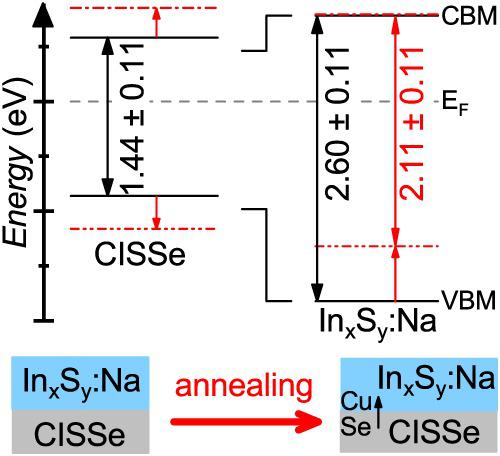
Doping an indium sulfide buffer layer with sodium is a promising route to replace the “state‐of‐the‐art” CdS buffer layer in chalcopyrite‐based thin‐film solar cells, as it achieves efficiencies as high as 17.9% for large‐area devices (30 cm × 30 cm). We report on the chemical and electronic structure of the InxSy:Na/CuIn(S,Se)2 (CISSe) interface for thin‐film solar cells by means of photoelectron, soft x‐ray emission, and inverse photoemission spectroscopy. For as‐deposited InxSy:Na buffer layers, we find a sulfur‐poor surface and, in comparison to undoped InxSy and the standard CdS buffer, derive a large electronic surface band gap of 2.60 ± 0.11 eV. The conduction band offset at the buffer/absorber interface is a spike of 0.32 ± 0.10 eV. After annealing at 200°C to simulate the thermal load of subsequent cell manufacturing processes, an additional diffusion of copper and selenium from the absorber towards the buffer layer surface is observed, leading to a distinct electronic surface band gap decrease of the InxSy:Na buffer layer (to 2.11 ± 0.11 eV). We speculate that the diffusion of absorber elements causes a band gap widening at the former absorber surface and that both effects lead to a reduction of the conduction band spike for the buried InxSy:Na/CISSe interface after annealing.
中文翻译:

通过Na掺杂缓冲层来提高性能-InxSy:Na / CuIn(S,Se)2薄膜太阳能电池界面的化学和电子结构
用钠掺杂硫化铟缓冲层是一种替代基于黄铜矿的薄膜太阳能电池中“最先进的” CdS缓冲层的有前途的途径,因为它可以实现高达17.9%的大面积效率设备(30厘米×30厘米)。我们通过光电子,软X射线发射和反光发射光谱法报告了薄膜太阳能电池的In x S y:Na / CuIn(S,Se)2(CISSe)接口的化学和电子结构。对于沉积的In x S y:Na缓冲层,我们发现了硫含量低的表面,并且与未掺杂的In x S y相比和标准CdS缓冲器,得出的电子表面带隙为2.60±0.11 eV。缓冲液/吸收剂界面的导带偏移为0.32±0.10 eV的尖峰。在200°C退火以模拟后续电池制造过程的热负荷后,观察到铜和硒从吸收体向缓冲层表面的额外扩散,导致In x S y的电子表面带隙明显减小:Na缓冲层(至2.11±0.11 eV)。我们推测吸收体元素的扩散会导致前一个吸收体表面的带隙变宽,并且这两种作用都会导致退火后掩埋的In x S y:Na / CISSe界面的导带峰减小。
更新日期:2018-02-09
中文翻译:
通过Na掺杂缓冲层来提高性能-InxSy:Na / CuIn(S,Se)2薄膜太阳能电池界面的化学和电子结构
用钠掺杂硫化铟缓冲层是一种替代基于黄铜矿的薄膜太阳能电池中“最先进的” CdS缓冲层的有前途的途径,因为它可以实现高达17.9%的大面积效率设备(30厘米×30厘米)。我们通过光电子,软X射线发射和反光发射光谱法报告了薄膜太阳能电池的In x S y:Na / CuIn(S,Se)2(CISSe)接口的化学和电子结构。对于沉积的In x S y:Na缓冲层,我们发现了硫含量低的表面,并且与未掺杂的In x S y相比和标准CdS缓冲器,得出的电子表面带隙为2.60±0.11 eV。缓冲液/吸收剂界面的导带偏移为0.32±0.10 eV的尖峰。在200°C退火以模拟后续电池制造过程的热负荷后,观察到铜和硒从吸收体向缓冲层表面的额外扩散,导致In x S y的电子表面带隙明显减小:Na缓冲层(至2.11±0.11 eV)。我们推测吸收体元素的扩散会导致前一个吸收体表面的带隙变宽,并且这两种作用都会导致退火后掩埋的In x S y:Na / CISSe界面的导带峰减小。


 京公网安备 11010802027423号