当前位置:
X-MOL 学术
›
Adv. Mater.
›
论文详情
Our official English website, www.x-mol.net, welcomes your feedback! (Note: you will need to create a separate account there.)
Large‐Area Atomic Layers of the Charge‐Density‐Wave Conductor TiSe2
Advanced Materials ( IF 29.4 ) Pub Date : 2018-01-10 , DOI: 10.1002/adma.201704382 Hong Wang 1, 2, 3 , Yu Chen 4 , Martial Duchamp 1 , Qingsheng Zeng 1 , Xuewen Wang 1 , Siu Hon Tsang 5 , Hongling Li 2 , Lin Jing 1 , Ting Yu 4 , Edwin Hang Tong Teo 1, 2, 3 , Zheng Liu 1
Advanced Materials ( IF 29.4 ) Pub Date : 2018-01-10 , DOI: 10.1002/adma.201704382 Hong Wang 1, 2, 3 , Yu Chen 4 , Martial Duchamp 1 , Qingsheng Zeng 1 , Xuewen Wang 1 , Siu Hon Tsang 5 , Hongling Li 2 , Lin Jing 1 , Ting Yu 4 , Edwin Hang Tong Teo 1, 2, 3 , Zheng Liu 1
Affiliation
|
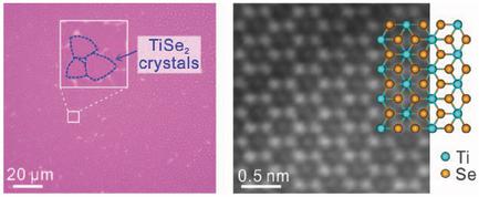
Layered transition metal (Ti, Ta, Nb, etc.) dichalcogenides are important prototypes for the study of the collective charge density wave (CDW). Reducing the system dimensionality is expected to lead to novel properties, as exemplified by the discovery of enhanced CDW order in ultrathin TiSe2. However, the syntheses of monolayer and large‐area 2D CDW conductors can currently only be achieved by molecular beam epitaxy under ultrahigh vacuum. This study reports the growth of monolayer crystals and up to 5 × 105 µm2 large films of the typical 2D CDW conductor—TiSe2—by ambient‐pressure chemical vapor deposition. Atomic resolution scanning transmission electron microscopy indicates the as‐grown samples are highly crystalline 1T‐phase TiSe2. Variable‐temperature Raman spectroscopy shows a CDW phase transition temperature of 212.5 K in few layer TiSe2, indicative of high crystal quality. This work not only allows the exploration of many‐body state of TiSe2 in 2D limit but also offers the possibility of utilizing large‐area TiSe2 in ultrathin electronic devices.
中文翻译:

电荷密度波导体TiSe2的大面积原子层
层状过渡金属(Ti,Ta,Nb等)二硫属化物是研究集体电荷密度波(CDW)的重要原型。降低系统尺寸预计会导致新的性能,例如在超薄TiSe 2中发现增强的CDW有序便可以证明这一点。但是,单层和大面积2D CDW导体的合成目前只能通过在超高真空下进行分子束外延来实现。这项研究报告了通过环境压力化学气相沉积法生长的典型2D CDW导体TiSe 2的单层晶体和最多5×10 5 µm 2的大薄膜。原子分辨率扫描透射电子显微镜表明所生长的样品为高度结晶的1T相TiSe2。可变温度拉曼光谱显示,在几层TiSe 2中,CDW相变温度为212.5 K ,表明晶体质量高。这项工作不仅允许在二维极限内探索TiSe 2的多体状态,而且还提供了在超薄电子设备中利用大面积TiSe 2的可能性。
更新日期:2018-01-10
中文翻译:
电荷密度波导体TiSe2的大面积原子层
层状过渡金属(Ti,Ta,Nb等)二硫属化物是研究集体电荷密度波(CDW)的重要原型。降低系统尺寸预计会导致新的性能,例如在超薄TiSe 2中发现增强的CDW有序便可以证明这一点。但是,单层和大面积2D CDW导体的合成目前只能通过在超高真空下进行分子束外延来实现。这项研究报告了通过环境压力化学气相沉积法生长的典型2D CDW导体TiSe 2的单层晶体和最多5×10 5 µm 2的大薄膜。原子分辨率扫描透射电子显微镜表明所生长的样品为高度结晶的1T相TiSe2。可变温度拉曼光谱显示,在几层TiSe 2中,CDW相变温度为212.5 K ,表明晶体质量高。这项工作不仅允许在二维极限内探索TiSe 2的多体状态,而且还提供了在超薄电子设备中利用大面积TiSe 2的可能性。


 京公网安备 11010802027423号