Our official English website, www.x-mol.net, welcomes your feedback! (Note: you will need to create a separate account there.)
Electrical Double Layer-Induced Ion Surface Accumulation for Ultrasensitive Refractive Index Sensing with Nanostructured Porous Silicon Interferometers
ACS Sensors ( IF 8.9 ) Pub Date : 2018-01-04 00:00:00 , DOI: 10.1021/acssensors.7b00650 Stefano Mariani 1 , Lucanos Marsilio Strambini 2 , Giuseppe Barillaro 1, 2
ACS Sensors ( IF 8.9 ) Pub Date : 2018-01-04 00:00:00 , DOI: 10.1021/acssensors.7b00650 Stefano Mariani 1 , Lucanos Marsilio Strambini 2 , Giuseppe Barillaro 1, 2
Affiliation
|
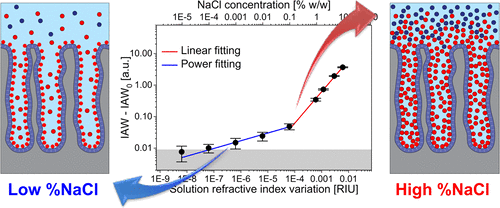
Herein, we provide the first experimental evidence on the use of electrical double layer (EDL)-induced accumulation of charged ions (using both Na+ and K+ ions in water as the model) onto a negatively charged nanostructured surface (e.g., thermally growth SiO2)—Ion Surface Accumulation, ISA—as a means of improving performance of nanostructured porous silicon (PSi) interferometers for optical refractometric applications. Nanostructured PSi interferometers are very promising optical platforms for refractive index sensing due to PSi huge specific surface (hundreds of m2 per gram) and low preparation cost (less than $0.01 per 8 in. silicon wafer), though they have shown poor resolution (R) and detection limit (DL) (on the order of 10–4–10–5 RIU) compared to other plasmonic and photonic platforms (R and DL on the order of 10–7–10–8 RIU). This can be ascribed to both low sensitivity and high noise floor of PSi interferometers when bulk refractive index variation of the solution infiltrating the nanopores either approaches or is below 10–4 RIU. Electrical double layer-induced ion surface accumulation (EDL-ISA) on oxidized PSi interferometers allows the interferometer output signal (spectral interferogram) to be impressively amplified at bulk refractive index variation below 10–4 RIU, increasing, in turn, sensitivity up to 2 orders of magnitude and allowing reliable measurement of refractive index variations to be carried out with both DL and R of 10–7 RIU. This represents a 250-fold-improvement (at least) with respect to the state-of-the-art literature on PSi refractometers and pushes PSi interferometer performance to that of state-of-the-art ultrasensitive photonics/plasmonics refractive index platforms.
中文翻译:

纳米结构多孔硅干涉仪用于超灵敏折射率传感的电双层诱导离子表面累积。
本文中,我们提供了第一个实验证据,证明使用电双层(EDL)诱导的带电离子积累(使用水中的Na +和K +离子作为模型)到带负电的纳米结构表面(例如,热生长) SiO 2)(离子表面累积,ISA)是一种改进用于光学折光测量应用的纳米结构多孔硅(PSi)干涉仪性能的方法。纳米结构的PSi干涉仪是非常有希望的用于折射率传感的光学平台,因为PSi的比表面积大(每克数百m 2)且制备成本低(每8英寸硅晶片少于0.01美元),尽管它们显示出较差的分辨率(R)和检测限(DL)(大约10 –4 –10 –5 RIU)(与其他等离子和光子平台相比)(R和DL大约10 –7 –10 –8 RIU)。当渗透到纳米孔中的溶液的整体折射率变化接近或低于10 –4 RIU时,这可以归因于PSi干涉仪的低灵敏度和高本底噪声。氧化的PSi干涉仪上的双电层诱导的离子表面累积(EDL-ISA)使干涉仪的输出信号(光谱干涉图)在整体折射率变化低于10 –4时得到显着放大RIU依次将灵敏度提高了2个数量级,并允许在DL和R均为10 – 7 RIU的情况下可靠地测量折射率变化。相对于有关PSi折光仪的最新文献,这表示(至少)提高了250倍,并将PSi干涉仪的性能推向了最新的超灵敏光子/等离子折光指数平台。
更新日期:2018-01-04
中文翻译:
纳米结构多孔硅干涉仪用于超灵敏折射率传感的电双层诱导离子表面累积。
本文中,我们提供了第一个实验证据,证明使用电双层(EDL)诱导的带电离子积累(使用水中的Na +和K +离子作为模型)到带负电的纳米结构表面(例如,热生长) SiO 2)(离子表面累积,ISA)是一种改进用于光学折光测量应用的纳米结构多孔硅(PSi)干涉仪性能的方法。纳米结构的PSi干涉仪是非常有希望的用于折射率传感的光学平台,因为PSi的比表面积大(每克数百m 2)且制备成本低(每8英寸硅晶片少于0.01美元),尽管它们显示出较差的分辨率(R)和检测限(DL)(大约10 –4 –10 –5 RIU)(与其他等离子和光子平台相比)(R和DL大约10 –7 –10 –8 RIU)。当渗透到纳米孔中的溶液的整体折射率变化接近或低于10 –4 RIU时,这可以归因于PSi干涉仪的低灵敏度和高本底噪声。氧化的PSi干涉仪上的双电层诱导的离子表面累积(EDL-ISA)使干涉仪的输出信号(光谱干涉图)在整体折射率变化低于10 –4时得到显着放大RIU依次将灵敏度提高了2个数量级,并允许在DL和R均为10 – 7 RIU的情况下可靠地测量折射率变化。相对于有关PSi折光仪的最新文献,这表示(至少)提高了250倍,并将PSi干涉仪的性能推向了最新的超灵敏光子/等离子折光指数平台。


 京公网安备 11010802027423号