当前位置:
X-MOL 学术
›
Nano Lett.
›
论文详情
Our official English website, www.x-mol.net, welcomes your feedback! (Note: you will need to create a separate account there.)
GaAs Nanowire pn-Junctions Produced by Low-Cost and High-Throughput Aerotaxy
Nano Letters ( IF 10.8 ) Pub Date : 2017-12-30 00:00:00 , DOI: 10.1021/acs.nanolett.7b04609 E. Barrigón 1, 2 , O. Hultin 2 , D. Lindgren 1 , F. Yadegari 1 , M. H. Magnusson 2 , L. Samuelson 1, 2 , L. I. M. Johansson 1 , M. T. Björk 1
Nano Letters ( IF 10.8 ) Pub Date : 2017-12-30 00:00:00 , DOI: 10.1021/acs.nanolett.7b04609 E. Barrigón 1, 2 , O. Hultin 2 , D. Lindgren 1 , F. Yadegari 1 , M. H. Magnusson 2 , L. Samuelson 1, 2 , L. I. M. Johansson 1 , M. T. Björk 1
Affiliation
|
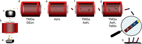
Semiconductor nanowires could significantly boost the functionality and performance of future electronics, light-emitting diodes, and solar cells. However, realizing this potential requires growth methods that enable high-throughput and low-cost production of nanowires with controlled doping. Aerotaxy is an aerosol-based method with extremely high growth rate that does not require a growth substrate, allowing mass-production of high-quality nanowires at a low cost. So far, pn-junctions, a crucial element of solar cells and light-emitting diodes, have not been realized by Aerotaxy growth. Here we report a further development of the Aerotaxy method and demonstrate the growth of GaAs nanowire pn-junctions. Our Aerotaxy system uses an aerosol generator for producing the catalytic seed particles, together with a growth reactor with multiple consecutive chambers for growth of material with different dopants. We show that the produced nanowire pn-junctions have excellent diode characteristics with a rectification ratio of >105, an ideality factor around 2, and very promising photoresponse. Using electron beam induced current and hyperspectral cathodoluminescence, we determined the location of the pn-junction and show that the grown nanowires have high doping levels, as well as electrical properties and diffusion lengths comparable to nanowires grown using metal organic vapor phase epitaxy. Our findings demonstrate that high-quality GaAs nanowire pn-junctions can be produced using a low-cost technique suitable for mass-production, paving the way for industrial-scale production of nanowire-based solar cells.
中文翻译:

低成本和高通量航空运动产生的GaAs纳米线pn结
半导体纳米线可以大大提高未来电子设备,发光二极管和太阳能电池的功能和性能。但是,要实现这一潜力,需要采用能够以受控的掺杂方式高产量,低成本地生产纳米线的生长方法。航迹法是一种基于气溶胶的方法,具有极高的生长速率,不需要生长基质,因此可以低成本大量生产高质量的纳米线。到目前为止,Aerotaxy的增长尚未实现pn结,这是太阳能电池和发光二极管的关键元素。在这里,我们报告了航空航天方法的进一步发展,并证明了GaAs纳米线pn结的增长。我们的Aerotaxy系统使用气溶胶发生器产生催化种子颗粒,以及具有多个连续腔室的生长反应器,用于生长具有不同掺杂剂的材料。我们表明,所生产的纳米线pn结具有出色的二极管特性,其整流比> 105,理想因数约为2,非常有前途的光响应。使用电子束感应电流和高光谱阴极发光,我们确定了pn结的位置,并表明与使用金属有机气相外延生长的纳米线相比,生长的纳米线具有较高的掺杂水平以及电学性质和扩散长度。我们的发现表明,可以使用适合批量生产的低成本技术来生产高质量的GaAs纳米线pn结,这为纳米线基太阳能电池的工业规模生产铺平了道路。
更新日期:2017-12-30
中文翻译:
低成本和高通量航空运动产生的GaAs纳米线pn结
半导体纳米线可以大大提高未来电子设备,发光二极管和太阳能电池的功能和性能。但是,要实现这一潜力,需要采用能够以受控的掺杂方式高产量,低成本地生产纳米线的生长方法。航迹法是一种基于气溶胶的方法,具有极高的生长速率,不需要生长基质,因此可以低成本大量生产高质量的纳米线。到目前为止,Aerotaxy的增长尚未实现pn结,这是太阳能电池和发光二极管的关键元素。在这里,我们报告了航空航天方法的进一步发展,并证明了GaAs纳米线pn结的增长。我们的Aerotaxy系统使用气溶胶发生器产生催化种子颗粒,以及具有多个连续腔室的生长反应器,用于生长具有不同掺杂剂的材料。我们表明,所生产的纳米线pn结具有出色的二极管特性,其整流比> 105,理想因数约为2,非常有前途的光响应。使用电子束感应电流和高光谱阴极发光,我们确定了pn结的位置,并表明与使用金属有机气相外延生长的纳米线相比,生长的纳米线具有较高的掺杂水平以及电学性质和扩散长度。我们的发现表明,可以使用适合批量生产的低成本技术来生产高质量的GaAs纳米线pn结,这为纳米线基太阳能电池的工业规模生产铺平了道路。


 京公网安备 11010802027423号