当前位置:
X-MOL 学术
›
Nano Lett.
›
论文详情
Our official English website, www.x-mol.net, welcomes your feedback! (Note: you will need to create a separate account there.)
Spatial Control of Multiphoton Electron Excitations in InAs Nanowires by Varying Crystal Phase and Light Polarization
Nano Letters ( IF 10.8 ) Pub Date : 2018-01-11 00:00:00 , DOI: 10.1021/acs.nanolett.7b04267 Erik Mårsell 1 , Emil Boström 1 , Anne Harth 1 , Arthur Losquin 1 , Chen Guo 1 , Yu-Chen Cheng 1 , Eleonora Lorek 1 , Sebastian Lehmann 1 , Gustav Nylund 1 , Martin Stankovski 1 , Cord L. Arnold 1 , Miguel Miranda 1 , Kimberly A. Dick 1 , Johan Mauritsson 1 , Claudio Verdozzi 1 , Anne L’Huillier 1 , Anders Mikkelsen 1
Nano Letters ( IF 10.8 ) Pub Date : 2018-01-11 00:00:00 , DOI: 10.1021/acs.nanolett.7b04267 Erik Mårsell 1 , Emil Boström 1 , Anne Harth 1 , Arthur Losquin 1 , Chen Guo 1 , Yu-Chen Cheng 1 , Eleonora Lorek 1 , Sebastian Lehmann 1 , Gustav Nylund 1 , Martin Stankovski 1 , Cord L. Arnold 1 , Miguel Miranda 1 , Kimberly A. Dick 1 , Johan Mauritsson 1 , Claudio Verdozzi 1 , Anne L’Huillier 1 , Anders Mikkelsen 1
Affiliation
|
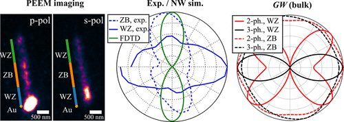
We demonstrate the control of multiphoton electron excitations in InAs nanowires (NWs) by altering the crystal structure and the light polarization. Using few-cycle, near-infrared laser pulses from an optical parametric chirped-pulse amplification system, we induce multiphoton electron excitations in InAs nanowires with controlled wurtzite (WZ) and zincblende (ZB) segments. With a photoemission electron microscope, we show that we can selectively induce multiphoton electron emission from WZ or ZB segments of the same wire by varying the light polarization. Developing ab initio GW calculations of first to third order multiphoton excitations and using finite-difference time-domain simulations, we explain the experimental findings: While the electric-field enhancement due to the semiconductor/vacuum interface has a similar effect for all NW segments, the second and third order multiphoton transitions in the band structure of WZ InAs are highly anisotropic in contrast to ZB InAs. As the crystal phase of NWs can be precisely and reliably tailored, our findings open up for new semiconductor optoelectronics with controllable nanoscale emission of electrons through vacuum or dielectric barriers.
中文翻译:

InAs纳米线上多光子电子激发的晶相和光偏振变化的空间控制
我们演示了通过改变晶体结构和光偏振来控制InAs纳米线(NWs)中的多光子电子激发。使用来自光学参量chi脉冲放大系统的短周期,近红外激光脉冲,我们在具有受控纤锌矿(WZ)和闪锌矿(ZB)段的InAs纳米线中诱导多光子电子激发。使用光发射电子显微镜,我们表明可以通过改变光的偏振选择性地诱导同一条线的WZ或ZB片段发出多光子电子。开发一阶至三阶多光子激发的从头算来GW计算并使用有限差分时域仿真,我们解释了实验结果:尽管由于半导体/真空界面而产生的电场增强对所有NW区段都有相似的影响,与ZB InAs相比,WZ InAs的能带结构中的二阶和三阶多光子跃迁具有高度的各向异性。由于可以精确可靠地定制NW的晶相,因此我们的发现为通过真空或介电势垒可控制的纳米级电子发射的新型半导体光电子打开了大门。
更新日期:2018-01-11
中文翻译:
InAs纳米线上多光子电子激发的晶相和光偏振变化的空间控制
我们演示了通过改变晶体结构和光偏振来控制InAs纳米线(NWs)中的多光子电子激发。使用来自光学参量chi脉冲放大系统的短周期,近红外激光脉冲,我们在具有受控纤锌矿(WZ)和闪锌矿(ZB)段的InAs纳米线中诱导多光子电子激发。使用光发射电子显微镜,我们表明可以通过改变光的偏振选择性地诱导同一条线的WZ或ZB片段发出多光子电子。开发一阶至三阶多光子激发的从头算来GW计算并使用有限差分时域仿真,我们解释了实验结果:尽管由于半导体/真空界面而产生的电场增强对所有NW区段都有相似的影响,与ZB InAs相比,WZ InAs的能带结构中的二阶和三阶多光子跃迁具有高度的各向异性。由于可以精确可靠地定制NW的晶相,因此我们的发现为通过真空或介电势垒可控制的纳米级电子发射的新型半导体光电子打开了大门。


 京公网安备 11010802027423号