当前位置:
X-MOL 学术
›
Adv. Mater. Interfaces
›
论文详情
Our official English website, www.x-mol.net, welcomes your feedback! (Note: you will need to create a separate account there.)
Atomic Layer Deposition of p‐Type Semiconducting Thin Films: a Review
Advanced Materials Interfaces ( IF 5.4 ) Pub Date : 2017-09-11 , DOI: 10.1002/admi.201700300 Tripurari Sharan Tripathi 1 , Maarit Karppinen 1
Advanced Materials Interfaces ( IF 5.4 ) Pub Date : 2017-09-11 , DOI: 10.1002/admi.201700300 Tripurari Sharan Tripathi 1 , Maarit Karppinen 1
Affiliation
|
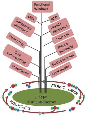
Semiconductors such as elemental silicon allowing both p‐type and n‐type doping are the backbone of the current microelectronics industry, while the continuous progress in fabrication techniques has been the key for ever‐increasing integration density and device miniaturization. Similarly, in the strongly emerging field of transparent electronics both p‐type and n‐type compound semiconductors are needed that moreover should be transparent within the entire visible spectral range. Atomic layer deposition (ALD) has been the thin‐film deposition method of choice for a number of challenging applications in microelectronics, and it would also be a highly relevant technology for transparent electronics. Currently the appropriate p‐type semiconducting compounds are far outnumbered by the n‐type compounds. Hence there is an obvious search for high‐quality thin films of new p‐type compound semiconductors. This is clearly seen in the increasing number of ALD papers published annualy on p‐type semiconducting materials. In this overview the current state of research in the field is briefly presented; the ALD processes so far developed for the various p‐type (transparent) conducting material candidates are summarized, and the most prominent electrical transport and optical properties achieved for these thin films are highlighted.
中文翻译:

p型半导体薄膜的原子层沉积:综述
允许同时进行p型和n型掺杂的元素硅等半导体是当前微电子行业的骨干,而制造技术的不断进步一直是不断提高集成度和缩小器件尺寸的关键。同样,在透明电子学这个新兴领域,p型和n型化合物半导体都需要,而且在整个可见光谱范围内都应该是透明的。原子层沉积(ALD)已经成为微电子学中许多具有挑战性的应用中选择的薄膜沉积方法,对于透明电子学来说,原子层沉积也是一项高度相关的技术。目前,合适的p型半导体化合物远远超过n型化合物。因此,显然在寻找新型p型化合物半导体的高质量薄膜。从每年发表的有关p型半导体材料的ALD论文数量不断增加中可以清楚地看出这一点。在此概述中,简要介绍了该领域的当前研究状态。总结了迄今为止为各种p型(透明)导电材料候选物开发的ALD工艺,并着重介绍了这些薄膜实现的最突出的电传输和光学性能。
更新日期:2017-09-11
中文翻译:
p型半导体薄膜的原子层沉积:综述
允许同时进行p型和n型掺杂的元素硅等半导体是当前微电子行业的骨干,而制造技术的不断进步一直是不断提高集成度和缩小器件尺寸的关键。同样,在透明电子学这个新兴领域,p型和n型化合物半导体都需要,而且在整个可见光谱范围内都应该是透明的。原子层沉积(ALD)已经成为微电子学中许多具有挑战性的应用中选择的薄膜沉积方法,对于透明电子学来说,原子层沉积也是一项高度相关的技术。目前,合适的p型半导体化合物远远超过n型化合物。因此,显然在寻找新型p型化合物半导体的高质量薄膜。从每年发表的有关p型半导体材料的ALD论文数量不断增加中可以清楚地看出这一点。在此概述中,简要介绍了该领域的当前研究状态。总结了迄今为止为各种p型(透明)导电材料候选物开发的ALD工艺,并着重介绍了这些薄膜实现的最突出的电传输和光学性能。


 京公网安备 11010802027423号