当前位置:
X-MOL 学术
›
ACS Appl. Mater. Interfaces
›
论文详情
Our official English website, www.x-mol.net, welcomes your feedback! (Note: you will need to create a separate account there.)
Shape-Uniform, High-Quality Monolayered MoS2 Crystals for Gate-Tunable Photoluminescence
ACS Applied Materials & Interfaces ( IF 9.5 ) Pub Date : 2017-11-21 00:00:00 , DOI: 10.1021/acsami.7b14189 Xiumei Zhang 1 , Haiyan Nan 1, 2 , Shaoqing Xiao 1 , Xi Wan 1 , Zhenhua Ni 2 , Xiaofeng Gu 1 , Kostya Ostrikov 3, 4
ACS Applied Materials & Interfaces ( IF 9.5 ) Pub Date : 2017-11-21 00:00:00 , DOI: 10.1021/acsami.7b14189 Xiumei Zhang 1 , Haiyan Nan 1, 2 , Shaoqing Xiao 1 , Xi Wan 1 , Zhenhua Ni 2 , Xiaofeng Gu 1 , Kostya Ostrikov 3, 4
Affiliation
|
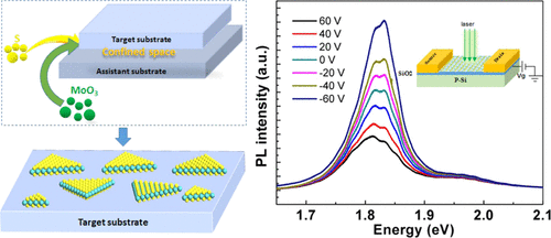
Two-dimensional molybdenum disulfide (MoS2) has recently drawn major attention due to its promising applications in electronics and optoelectronics. Chemical vapor deposition (CVD) is a scalable method to produce large-area MoS2 monolayers, yet it is challenging to achieve shape-uniform, high-quality monolayered MoS2 grains as random, diverse crystallographic orientations and various shapes are produced in the same CVD process. Here, we report the growth of high-quality MoS2 monolayers with uniform triangular shapes dominating (up to 89%) over other shapes on both SiO2/Si and sapphire substrates. The new confined-space CVD process prevents contamination and helps regulate the Mo/S ratio during the deposition. The as-grown triangular MoS2 monolayers exhibit grain sizes up to 150 μm and possess better crystalline properties and lighter n-type doping concentration than those of the monolayers grown by common CVD methods. The corresponding field effect transistor devices show high electron mobilities of 50–60 cm2 V–1 s–1 and positive threshold voltages of 21–35 V. This mild n-type behavior makes it possible to regulate the formation of excitons by back-gate voltage due to the interaction of excitons with free charge carriers in the MoS2 channel. As a result, gate-tunable photoluminescence (PL) effect, which is rarely achievable for MoS2 samples prepared by common CVD or mechanical exfoliation, is demonstrated. This study provides a simple versatile approach to fabricating monolayered crystals of MoS2 and other high-quality transition metal dichalcogenides and could lead to new optoelectronic devices based on gate-tunable PL effect.
中文翻译:

形状均匀,高质量的单层MoS 2晶体,可用于门可调的光致发光
由于二维二硫化钼(MoS 2)在电子和光电子领域的应用前景广阔,因此最近受到了广泛的关注。化学气相沉积(CVD)是生产大面积MoS 2单层的可扩展方法,但是要获得形状均匀,高质量的单层MoS 2晶粒却具有挑战性,因为随机,多样的晶体取向和相同形状都可以产生CVD工艺。在这里,我们报告了在两个SiO 2上均具有高品质的MoS 2单层的增长,这些三角形具有均匀的三角形形状(最多达89%),超过其他形状/ Si和蓝宝石衬底。新的密闭空间CVD工艺可防止污染,并有助于在沉积过程中调节Mo / S比。所生长的三角形MoS 2单层与通过常规CVD方法生长的单层相比,具有最大150μm的晶粒尺寸,并具有更好的结晶特性和更轻的n型掺杂浓度。相应的场效应晶体管器件显示出50–60 cm 2 V –1 s –1的高电子迁移率和21–35 V的正阈值电压。这种温和的n型行为使得可以通过反激来调节激子的形成。 MoS 2中激子与自由电荷载流子相互作用产生的栅极电压渠道。结果,证明了通过普通CVD或机械剥离法制备的MoS 2样品极难实现的栅极可调光致发光(PL)效果。这项研究提供了一种简单的通用方法来制造MoS 2和其他高质量过渡金属二卤化硅的单层晶体,并可能导致基于栅极可调PL效应的新型光电器件。
更新日期:2017-11-21
中文翻译:
形状均匀,高质量的单层MoS 2晶体,可用于门可调的光致发光
由于二维二硫化钼(MoS 2)在电子和光电子领域的应用前景广阔,因此最近受到了广泛的关注。化学气相沉积(CVD)是生产大面积MoS 2单层的可扩展方法,但是要获得形状均匀,高质量的单层MoS 2晶粒却具有挑战性,因为随机,多样的晶体取向和相同形状都可以产生CVD工艺。在这里,我们报告了在两个SiO 2上均具有高品质的MoS 2单层的增长,这些三角形具有均匀的三角形形状(最多达89%),超过其他形状/ Si和蓝宝石衬底。新的密闭空间CVD工艺可防止污染,并有助于在沉积过程中调节Mo / S比。所生长的三角形MoS 2单层与通过常规CVD方法生长的单层相比,具有最大150μm的晶粒尺寸,并具有更好的结晶特性和更轻的n型掺杂浓度。相应的场效应晶体管器件显示出50–60 cm 2 V –1 s –1的高电子迁移率和21–35 V的正阈值电压。这种温和的n型行为使得可以通过反激来调节激子的形成。 MoS 2中激子与自由电荷载流子相互作用产生的栅极电压渠道。结果,证明了通过普通CVD或机械剥离法制备的MoS 2样品极难实现的栅极可调光致发光(PL)效果。这项研究提供了一种简单的通用方法来制造MoS 2和其他高质量过渡金属二卤化硅的单层晶体,并可能导致基于栅极可调PL效应的新型光电器件。


 京公网安备 11010802027423号