当前位置:
X-MOL 学术
›
ACS Appl. Mater. Interfaces
›
论文详情
Our official English website, www.x-mol.net, welcomes your feedback! (Note: you will need to create a separate account there.)
Lead Halide Perovskites as Charge Generation Layers for Electron Mobility Measurement in Organic Semiconductors
ACS Applied Materials & Interfaces ( IF 9.5 ) Pub Date : 2017-11-17 00:00:00 , DOI: 10.1021/acsami.7b10361 John A. Love 1 , Markus Feuerstein 1 , Christian M. Wolff 1 , Antonio Facchetti 2 , Dieter Neher 1
ACS Applied Materials & Interfaces ( IF 9.5 ) Pub Date : 2017-11-17 00:00:00 , DOI: 10.1021/acsami.7b10361 John A. Love 1 , Markus Feuerstein 1 , Christian M. Wolff 1 , Antonio Facchetti 2 , Dieter Neher 1
Affiliation
|
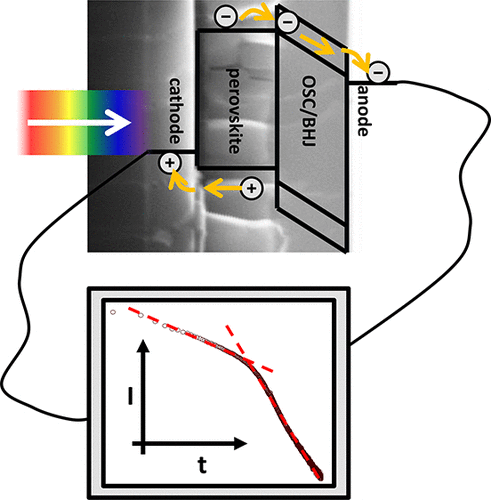
Hybrid lead halide perovskites are introduced as charge generation layers (CGLs) for the accurate determination of electron mobilities in thin organic semiconductors. Such hybrid perovskites have become a widely studied photovoltaic material in their own right, for their high efficiencies, ease of processing from solution, strong absorption, and efficient photogeneration of charge. Time-of-flight (ToF) measurements on bilayer samples consisting of the perovskite CGL and an organic semiconductor layer of different thickness are shown to be determined by the carrier motion through the organic material, consistent with the much higher charge carrier mobility in the perovskite. Together with the efficient photon-to-electron conversion in the perovskite, this high mobility imbalance enables electron-only mobility measurement on relatively thin application-relevant organic films, which would not be possible with traditional ToF measurements. This architecture enables electron-selective mobility measurements in single components as well as bulk-heterojunction films as demonstrated in the prototypical polymer/fullerene blends. To further demonstrate the potential of this approach, electron mobilities were measured as a function of electric field and temperature in an only 127 nm thick layer of a prototypical electron-transporting perylene diimide-based polymer, and found to be consistent with an exponential trap distribution of ca. 60 meV. Our study furthermore highlights the importance of high mobility charge transporting layers when designing perovskite solar cells.
中文翻译:

卤化钙钛矿作为有机半导体中电子迁移率测量的电荷产生层
杂化卤化钙钛矿被引入为电荷产生层(CGL),用于精确测定薄有机半导体中的电子迁移率。这种杂化钙钛矿凭借其高效率,易于从溶液中加工,强吸收性和高效的电荷光生化等优点,已成为一种广泛研究的光伏材料。钙钛矿CGL和不同厚度的有机半导体层组成的双层样品的飞行时间(ToF)测量显示是由穿过有机材料的载流子运动确定的,这与钙钛矿中高得多的电荷载流子迁移率一致。加上钙钛矿中有效的光子到电子的转换,这种高迁移率不平衡使得能够在相对薄的与应用相关的有机薄膜上进行纯电子迁移率测量,而这是传统ToF测量无法实现的。这种体系结构可以测量单个组分以及本体-异质结薄膜中的电子选择性迁移率,如典型的聚合物/富勒烯共混物中所示。为了进一步证明这种方法的潜力,在典型的电子传输per二酰亚胺基聚合物的仅127 nm厚的层中,将电子迁移率作为电场和温度的函数进行了测量,并发现它与指数陷阱分布一致约。60兆电子伏。我们的研究进一步强调了在设计钙钛矿太阳能电池时高迁移率电荷传输层的重要性。传统的ToF测量不可能做到这一点。这种体系结构可以测量单个组分以及本体-异质结薄膜中的电子选择性迁移率,如典型的聚合物/富勒烯共混物所示。为了进一步证明这种方法的潜力,在典型的电子传输per二酰亚胺基聚合物的仅127 nm厚的层中,将电子迁移率作为电场和温度的函数进行了测量,并发现它与指数陷阱分布一致约。60兆电子伏。我们的研究进一步强调了在设计钙钛矿太阳能电池时高迁移率电荷传输层的重要性。传统的ToF测量不可能做到这一点。这种体系结构可以测量单个组分以及本体-异质结薄膜中的电子选择性迁移率,如典型的聚合物/富勒烯共混物所示。为了进一步证明这种方法的潜力,在典型的电子传输per二酰亚胺基聚合物的仅127 nm厚的层中,将电子迁移率作为电场和温度的函数进行了测量,并发现它与指数陷阱分布一致约。60兆电子伏。我们的研究进一步强调了在设计钙钛矿太阳能电池时高迁移率电荷传输层的重要性。这种体系结构可以测量单个组分以及本体-异质结薄膜中的电子选择性迁移率,如典型的聚合物/富勒烯共混物所示。为了进一步证明这种方法的潜力,在典型的电子传输per二酰亚胺基聚合物的仅127 nm厚的层中,将电子迁移率作为电场和温度的函数进行了测量,并发现它与指数陷阱分布一致约。60兆电子伏。我们的研究进一步强调了在设计钙钛矿太阳能电池时高迁移率电荷传输层的重要性。这种体系结构可以测量单个组分以及本体-异质结薄膜中的电子选择性迁移率,如典型的聚合物/富勒烯共混物所示。为了进一步证明这种方法的潜力,在典型的电子传输per二酰亚胺基聚合物的仅127 nm厚的层中,将电子迁移率作为电场和温度的函数进行了测量,并发现它与指数陷阱分布一致约。60兆电子伏。我们的研究进一步强调了在设计钙钛矿太阳能电池时高迁移率电荷传输层的重要性。在典型的电子传输per二酰亚胺基聚合物的仅127 nm厚的层中,测量到的电子迁移率是电场和温度的函数,并且发现其与ca的指数陷阱分布一致。60兆电子伏。我们的研究进一步强调了在设计钙钛矿太阳能电池时高迁移率电荷传输层的重要性。在典型的电子传输per二酰亚胺基聚合物的仅127 nm厚的层中,测量到的电子迁移率是电场和温度的函数,并且发现其与ca的指数陷阱分布一致。60兆电子伏。我们的研究进一步强调了在设计钙钛矿太阳能电池时高迁移率电荷传输层的重要性。
更新日期:2017-11-19
中文翻译:
卤化钙钛矿作为有机半导体中电子迁移率测量的电荷产生层
杂化卤化钙钛矿被引入为电荷产生层(CGL),用于精确测定薄有机半导体中的电子迁移率。这种杂化钙钛矿凭借其高效率,易于从溶液中加工,强吸收性和高效的电荷光生化等优点,已成为一种广泛研究的光伏材料。钙钛矿CGL和不同厚度的有机半导体层组成的双层样品的飞行时间(ToF)测量显示是由穿过有机材料的载流子运动确定的,这与钙钛矿中高得多的电荷载流子迁移率一致。加上钙钛矿中有效的光子到电子的转换,这种高迁移率不平衡使得能够在相对薄的与应用相关的有机薄膜上进行纯电子迁移率测量,而这是传统ToF测量无法实现的。这种体系结构可以测量单个组分以及本体-异质结薄膜中的电子选择性迁移率,如典型的聚合物/富勒烯共混物中所示。为了进一步证明这种方法的潜力,在典型的电子传输per二酰亚胺基聚合物的仅127 nm厚的层中,将电子迁移率作为电场和温度的函数进行了测量,并发现它与指数陷阱分布一致约。60兆电子伏。我们的研究进一步强调了在设计钙钛矿太阳能电池时高迁移率电荷传输层的重要性。传统的ToF测量不可能做到这一点。这种体系结构可以测量单个组分以及本体-异质结薄膜中的电子选择性迁移率,如典型的聚合物/富勒烯共混物所示。为了进一步证明这种方法的潜力,在典型的电子传输per二酰亚胺基聚合物的仅127 nm厚的层中,将电子迁移率作为电场和温度的函数进行了测量,并发现它与指数陷阱分布一致约。60兆电子伏。我们的研究进一步强调了在设计钙钛矿太阳能电池时高迁移率电荷传输层的重要性。传统的ToF测量不可能做到这一点。这种体系结构可以测量单个组分以及本体-异质结薄膜中的电子选择性迁移率,如典型的聚合物/富勒烯共混物所示。为了进一步证明这种方法的潜力,在典型的电子传输per二酰亚胺基聚合物的仅127 nm厚的层中,将电子迁移率作为电场和温度的函数进行了测量,并发现它与指数陷阱分布一致约。60兆电子伏。我们的研究进一步强调了在设计钙钛矿太阳能电池时高迁移率电荷传输层的重要性。这种体系结构可以测量单个组分以及本体-异质结薄膜中的电子选择性迁移率,如典型的聚合物/富勒烯共混物所示。为了进一步证明这种方法的潜力,在典型的电子传输per二酰亚胺基聚合物的仅127 nm厚的层中,将电子迁移率作为电场和温度的函数进行了测量,并发现它与指数陷阱分布一致约。60兆电子伏。我们的研究进一步强调了在设计钙钛矿太阳能电池时高迁移率电荷传输层的重要性。这种体系结构可以测量单个组分以及本体-异质结薄膜中的电子选择性迁移率,如典型的聚合物/富勒烯共混物所示。为了进一步证明这种方法的潜力,在典型的电子传输per二酰亚胺基聚合物的仅127 nm厚的层中,将电子迁移率作为电场和温度的函数进行了测量,并发现它与指数陷阱分布一致约。60兆电子伏。我们的研究进一步强调了在设计钙钛矿太阳能电池时高迁移率电荷传输层的重要性。在典型的电子传输per二酰亚胺基聚合物的仅127 nm厚的层中,测量到的电子迁移率是电场和温度的函数,并且发现其与ca的指数陷阱分布一致。60兆电子伏。我们的研究进一步强调了在设计钙钛矿太阳能电池时高迁移率电荷传输层的重要性。在典型的电子传输per二酰亚胺基聚合物的仅127 nm厚的层中,测量到的电子迁移率是电场和温度的函数,并且发现其与ca的指数陷阱分布一致。60兆电子伏。我们的研究进一步强调了在设计钙钛矿太阳能电池时高迁移率电荷传输层的重要性。


 京公网安备 11010802027423号