Our official English website, www.x-mol.net, welcomes your feedback! (Note: you will need to create a separate account there.)
On-Chip Sorting of Long Semiconducting Carbon Nanotubes for Multiple Transistors along an Identical Array
ACS Nano ( IF 17.1 ) Pub Date : 2017-11-13 00:00:00 , DOI: 10.1021/acsnano.7b06282 Keigo Otsuka 1 , Taiki Inoue 1 , Etsuo Maeda 1 , Reo Kometani 1 , Shohei Chiashi 1 , Shigeo Maruyama 1, 2
ACS Nano ( IF 17.1 ) Pub Date : 2017-11-13 00:00:00 , DOI: 10.1021/acsnano.7b06282 Keigo Otsuka 1 , Taiki Inoue 1 , Etsuo Maeda 1 , Reo Kometani 1 , Shohei Chiashi 1 , Shigeo Maruyama 1, 2
Affiliation
|
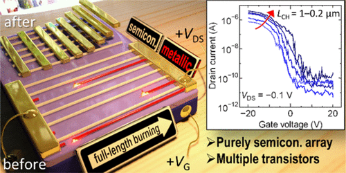
Ballistic transport and sub-10 nm channel lengths have been achieved in transistors containing one single-walled carbon nanotube (SWNT). To fill the gap between single-tube transistors and high-performance logic circuits for the replacement of silicon, large-area, high-density, and purely semiconducting (s-) SWNT arrays are highly desired. Here we demonstrate the fabrication of multiple transistors along a purely semiconducting SWNT array via an on-chip purification method. Water- and polymer-assisted burning from site-controlled nanogaps is developed for the reliable full-length removal of metallic SWNTs with the damage to s-SWNTs minimized even in high-density arrays. All the transistors with various channel lengths show large on-state current and excellent switching behavior in the off-state. Since our method potentially provides pure s-SWNT arrays over a large area with negligible damage, numerous transistors with arbitrary dimensions could be fabricated using a conventional semiconductor process, leading to SWNT-based logic, high-speed communication, and other next-generation electronic devices.
中文翻译:

沿相同阵列的多个晶体管的长半导体碳纳米管的片内分选
在包含一个单壁碳纳米管(SWNT)的晶体管中,已经实现了弹道传输和低于10 nm的沟道长度。为了填补单管晶体管和高性能逻辑电路之间的空白以替代硅,迫切需要大面积,高密度和纯半导体(s-)SWNT阵列。在这里,我们演示了通过一个纯半导体SWNT阵列通过以下方式制造多个晶体管的过程:片上纯化方法。通过现场控制的纳米间隙进行水和聚合物辅助燃烧,可以可靠地全长去除金属单壁碳纳米管,即使在高密度阵列中,对s-SWNT的破坏也可以最小化。具有各种沟道长度的所有晶体管在截止状态下均显示出大的导通状态电流和出色的开关性能。由于我们的方法有可能在大面积上提供纯s-SWNT阵列,而损害可忽略不计,因此可以使用常规半导体工艺制造具有任意尺寸的众多晶体管,从而实现基于SWNT的逻辑,高速通信和其他下一代电子技术设备。
更新日期:2017-11-14
中文翻译:
沿相同阵列的多个晶体管的长半导体碳纳米管的片内分选
在包含一个单壁碳纳米管(SWNT)的晶体管中,已经实现了弹道传输和低于10 nm的沟道长度。为了填补单管晶体管和高性能逻辑电路之间的空白以替代硅,迫切需要大面积,高密度和纯半导体(s-)SWNT阵列。在这里,我们演示了通过一个纯半导体SWNT阵列通过以下方式制造多个晶体管的过程:片上纯化方法。通过现场控制的纳米间隙进行水和聚合物辅助燃烧,可以可靠地全长去除金属单壁碳纳米管,即使在高密度阵列中,对s-SWNT的破坏也可以最小化。具有各种沟道长度的所有晶体管在截止状态下均显示出大的导通状态电流和出色的开关性能。由于我们的方法有可能在大面积上提供纯s-SWNT阵列,而损害可忽略不计,因此可以使用常规半导体工艺制造具有任意尺寸的众多晶体管,从而实现基于SWNT的逻辑,高速通信和其他下一代电子技术设备。


 京公网安备 11010802027423号