当前位置:
X-MOL 学术
›
Adv. Electron. Mater.
›
论文详情
Our official English website, www.x-mol.net, welcomes your feedback! (Note: you will need to create a separate account there.)
Surface State Mediated Interlayer Excitons in a 2D Nonlayered–Layered Semiconductor Heterojunction
Advanced Electronic Materials ( IF 6.2 ) Pub Date : 2017-10-30 , DOI: 10.1002/aelm.201700373 Liyun Zhao 1, 2 , Xuewen Wang 3 , Zhepeng Zhang 2, 4 , Pengfei Yang 2 , Jie Chen 2, 5 , Yanqi Chen 2 , Hao Wang 2 , Qiuyu Shang 2 , Yuyang Zhang 6 , Yanfeng Zhang 2, 4 , Xinfeng Liu 5 , Jiancai Leng 1 , Zheng Liu 3 , Qing Zhang 2
Advanced Electronic Materials ( IF 6.2 ) Pub Date : 2017-10-30 , DOI: 10.1002/aelm.201700373 Liyun Zhao 1, 2 , Xuewen Wang 3 , Zhepeng Zhang 2, 4 , Pengfei Yang 2 , Jie Chen 2, 5 , Yanqi Chen 2 , Hao Wang 2 , Qiuyu Shang 2 , Yuyang Zhang 6 , Yanfeng Zhang 2, 4 , Xinfeng Liu 5 , Jiancai Leng 1 , Zheng Liu 3 , Qing Zhang 2
Affiliation
|
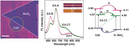
Van der Waals heterojunctions of 2D layered semiconductors and nonlayered technological important II–V semiconductors provide unprecedented opportunities to engineer exciton and carrier dynamics in 2D optoelectronic devices. However, fabrication of such artificial heterojunctions with type‐II band alignment structure and realization of interlayer excitons is challenging. Here, CdS–MoS2 type‐II heterojunctions vertically stacked with few layered MoS2 and ultrathin CdS film are reported. Steady‐state spectroscopy and time‐resolved photoluminescence spectroscopy are used to study exciton and carrier dynamics in these heterojunctions. The surface states of the ultrathin CdS film caused by dangling bonds mediate interlayer exciton emission located at 753 nm in a CdS–bilayer MoS2 heterojunction via charge transition between the MoS2 indirect band and the CdS valence band. As a contrast, the surface states of CdS impede the recombination of interlayer excitons in a CdS‐monolayer MoS2 heterojunction. These results are helpful for development of high‐performance ultrathin optoelectronic and energy devices including light emission diodes, solar cells, and photodetectors.
中文翻译:

二维非分层半导体异质结中的表面状态介导的层间激子
2D层状半导体和非层状重要II-V半导体的Van der Waals异质结为工程设计2D光电器件中的激子和载流子动力学提供了前所未有的机会。然而,具有II型能带对准结构的人工异质结的制造以及层间激子的实现具有挑战性。此处报道了垂直堆叠的CdS–MoS 2 type-II异质结,几乎没有分层的MoS 2和超薄CdS膜。稳态光谱学和时间分辨光致发光光谱学用于研究这些异质结中的激子和载流子动力学。悬空键引起的超薄CdS薄膜的表面状态介导了CdS-双层MoS中位于753 nm的层间激子发射通过在MoS 2间接带和CdS价带之间进行电荷跃迁来形成2异质结。相比之下,CdS的表面态阻碍了CdS-单层MoS 2异质结中层间激子的重组。这些结果有助于开发高性能超薄光电和能源设备,包括发光二极管,太阳能电池和光电探测器。
更新日期:2017-10-30
中文翻译:
二维非分层半导体异质结中的表面状态介导的层间激子
2D层状半导体和非层状重要II-V半导体的Van der Waals异质结为工程设计2D光电器件中的激子和载流子动力学提供了前所未有的机会。然而,具有II型能带对准结构的人工异质结的制造以及层间激子的实现具有挑战性。此处报道了垂直堆叠的CdS–MoS 2 type-II异质结,几乎没有分层的MoS 2和超薄CdS膜。稳态光谱学和时间分辨光致发光光谱学用于研究这些异质结中的激子和载流子动力学。悬空键引起的超薄CdS薄膜的表面状态介导了CdS-双层MoS中位于753 nm的层间激子发射通过在MoS 2间接带和CdS价带之间进行电荷跃迁来形成2异质结。相比之下,CdS的表面态阻碍了CdS-单层MoS 2异质结中层间激子的重组。这些结果有助于开发高性能超薄光电和能源设备,包括发光二极管,太阳能电池和光电探测器。


 京公网安备 11010802027423号