当前位置:
X-MOL 学术
›
Adv. Electron. Mater.
›
论文详情
Our official English website, www.x-mol.net, welcomes your feedback! (Note: you will need to create a separate account there.)
Ambipolar Organic Field‐Effect Transistors Based on a Dual‐Function, Ultrathin and Highly Crystalline 2,9‐didecyldinaphtho[2,3‐b:2′,3′‐f]thieno[3,2‐b]thiophene (C10‐DNTT) Layer
Advanced Electronic Materials ( IF 6.2 ) Pub Date : 2017-10-11 , DOI: 10.1002/aelm.201700268 Shuyun Huang 1 , Boyu Peng 1 , Paddy Kwok Leung Chan 1
Advanced Electronic Materials ( IF 6.2 ) Pub Date : 2017-10-11 , DOI: 10.1002/aelm.201700268 Shuyun Huang 1 , Boyu Peng 1 , Paddy Kwok Leung Chan 1
Affiliation
|
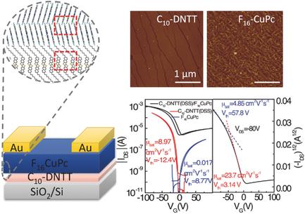
Ultrathin organic semiconductor thin films have great value in the investigation of carrier transport behavior in organic field‐effect transistors (OFETs). Here, the dual solution shearing (DSS) method is adopted to deposit ultrathin and closely packed 2,9‐didecyldinaphtho[2,3‐b:2′,3′‐f]thieno[3,2‐b]thiophene (C10‐DNTT) films. This smooth, ultrathin and highly crystalline DSS‐processed C10‐DNTT layer can be utilized in p–n stacking bilayer ambipolar OFETs. It has two major functions in the bilayer OFET: (i) it acts as the p‐channel active layer; and (ii) it serves as the growth template of the upper n‐type semiconductor layer. The closely packed alkyl side chains of the C10‐DNTT molecules behave like long alkyl chains in the self‐assembled monolayer and can assist the packing and orientation of the following layer. The F16CuPc layer grown on DSS‐processed C10‐DNTT shows crystallized lamellae structure. The smooth C10‐DNTT surface can suppress the trap states and enhance the charge transfer between the p–n layer interface. The drain‐source current (IDS) in the p‐channel and n‐channel shows a threefold and fivefold increase compared with two‐step thermal evaporation. These findings demonstrate the potential of using solution‐processed ultrathin organic semiconductor in multilayer organic electronics, which cannot be easily achieved by the conventional thermal evaporation approach.
中文翻译:

基于双功能,超薄和高度结晶的2,9-二癸基二萘并[2,3-b:2′,3'-f]噻吩并[3,2-b]噻吩的双极有机场效应晶体管(C10-DNTT ) 层
超薄有机半导体薄膜在研究有机场效应晶体管(OFET)中的载流子传输行为方面具有重要价值。在这里,采用双溶液剪切(DSS)方法沉积超薄且紧密堆积的2,9-二癸基萘并[2,3-b:2',3'-f]噻吩并[3,2-b]噻吩(C 10 ‐DNTT)电影。这种光滑,超薄且高度结晶的DSS处理的C 10 -DNTT层可用于p–n堆叠双层双极性OFET中。它在双层OFET中具有两个主要功能:(i)充当p通道有源层;(ii)用作上部n型半导体层的生长模板。C 10的紧密堆积的烷基侧链‐DNTT分子在自组装单层中的行为类似于长烷基链,可以帮助下一层的堆积和定向。在DSS处理的C 10 -DNTT上生长的F 16 CuPc层显示出结晶的片状结构。光滑的C 10 ‐DNTT表面可以抑制陷阱态并增强p–n层界面之间的电荷转移。与两步热蒸发相比,p沟道和n沟道中的漏极-源极电流(I DS)分别增加了三倍和五倍。这些发现证明了在多层有机电子产品中使用溶液处理的超薄有机半导体的潜力,这是传统的热蒸发方法无法轻易实现的。
更新日期:2017-10-11
中文翻译:
基于双功能,超薄和高度结晶的2,9-二癸基二萘并[2,3-b:2′,3'-f]噻吩并[3,2-b]噻吩的双极有机场效应晶体管(C10-DNTT ) 层
超薄有机半导体薄膜在研究有机场效应晶体管(OFET)中的载流子传输行为方面具有重要价值。在这里,采用双溶液剪切(DSS)方法沉积超薄且紧密堆积的2,9-二癸基萘并[2,3-b:2',3'-f]噻吩并[3,2-b]噻吩(C 10 ‐DNTT)电影。这种光滑,超薄且高度结晶的DSS处理的C 10 -DNTT层可用于p–n堆叠双层双极性OFET中。它在双层OFET中具有两个主要功能:(i)充当p通道有源层;(ii)用作上部n型半导体层的生长模板。C 10的紧密堆积的烷基侧链‐DNTT分子在自组装单层中的行为类似于长烷基链,可以帮助下一层的堆积和定向。在DSS处理的C 10 -DNTT上生长的F 16 CuPc层显示出结晶的片状结构。光滑的C 10 ‐DNTT表面可以抑制陷阱态并增强p–n层界面之间的电荷转移。与两步热蒸发相比,p沟道和n沟道中的漏极-源极电流(I DS)分别增加了三倍和五倍。这些发现证明了在多层有机电子产品中使用溶液处理的超薄有机半导体的潜力,这是传统的热蒸发方法无法轻易实现的。


 京公网安备 11010802027423号