Nano-Micro Letters ( IF 26.6 ) Pub Date : 2017-08-16 , DOI: 10.1007/s40820-017-0153-5 Wei Wang 1 , Liang Wang 1 , Gaole Dai 1 , Wei Deng 1 , Xiujuan Zhang 1 , Jiansheng Jie 1 , Xiaohong Zhang 1
|
Abstract
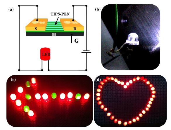
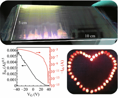
Organic field-effect transistors (OFETs) based on organic micro-/nanocrystals have been widely reported with charge carrier mobility exceeding 1.0 cm2 V−1 s−1, demonstrating great potential for high-performance, low-cost organic electronic applications. However, fabrication of large-area organic micro-/nanocrystal arrays with consistent crystal growth direction has posed a significant technical challenge. Here, we describe a solution-processed dip-coating technique to grow large-area, aligned 9,10-bis(phenylethynyl) anthracene (BPEA) and 6,13-bis(triisopropylsilylethynyl) pentacene (TIPS-PEN) single-crystalline nanoribbon arrays. The method is scalable to a 5 × 10 cm2 wafer substrate, with around 60% of the wafer surface covered by aligned crystals. The quality of crystals can be easily controlled by tuning the dip-coating speed. Furthermore, OFETs based on well-aligned BPEA and TIPS-PEN single-crystalline nanoribbons were constructed. By optimizing channel lengths and using appropriate metallic electrodes, the BPEA and TIPS-PEN-based OFETs showed hole mobility exceeding 2.0 cm2 V−1 s−1 (average mobility 1.2 cm2 V−1 s−1) and 3.0 cm2 V−1 s−1 (average mobility 2.0 cm2 V−1 s−1), respectively. They both have a high on/off ratio (I on/I off) > 109. The performance can well satisfy the requirements for light-emitting diodes driving.
Graphical Abstract
中文翻译:
用于晶体管和发光二极管驱动的大面积排列单晶有机纳米带阵列的可控生长
摘要
基于有机微/纳米晶体的有机场效应晶体管 (OFET) 已被广泛报道,其电荷载流子迁移率超过 1.0 cm 2 V -1 s -1,在高性能、低成本的有机电子应用中显示出巨大的潜力。然而,具有一致晶体生长方向的大面积有机微/纳米晶体阵列的制造提出了重大的技术挑战。在这里,我们描述了一种溶液处理浸涂技术来生长大面积、对齐的 9,10-双(苯乙炔基)蒽(BPEA)和 6,13-双(三异丙基甲硅烷基乙炔基)并五苯(TIPS-PEN)单晶纳米带数组。该方法可扩展到 5 × 10 cm 2晶圆基板,约 60% 的晶圆表面被排列整齐的晶体覆盖。通过调整浸涂速度可以很容易地控制晶体的质量。此外,构建了基于良好排列的 BPEA 和 TIPS-PEN 单晶纳米带的 OFET。通过优化沟道长度和使用合适的金属电极,基于 BPEA 和 TIPS-PEN 的 OFET 显示出超过 2.0 cm 2 V -1 s -1(平均迁移率 1.2 cm 2 V -1 s -1)和 3.0 cm 2 V的空穴迁移率-1 s -1 (平均迁移率 2.0 cm 2 V -1 s -1), 分别。它们都有很高的开/关比(I on / I off)> 10 9。性能可以很好地满足发光二极管驱动的要求。
图形概要


 京公网安备 11010802027423号