当前位置:
X-MOL 学术
›
Nano Lett.
›
论文详情
Our official English website, www.x-mol.net, welcomes your feedback! (Note: you will need to create a separate account there.)
Hybrid Integration of Solid-State Quantum Emitters on a Silicon Photonic Chip
Nano Letters ( IF 10.8 ) Pub Date : 2017-11-17 00:00:00 , DOI: 10.1021/acs.nanolett.7b03220 Je-Hyung Kim 1, 2 , Shahriar Aghaeimeibodi 1 , Christopher J. K. Richardson 3 , Richard P. Leavitt 3 , Dirk Englund 4 , Edo Waks 1, 5
Nano Letters ( IF 10.8 ) Pub Date : 2017-11-17 00:00:00 , DOI: 10.1021/acs.nanolett.7b03220 Je-Hyung Kim 1, 2 , Shahriar Aghaeimeibodi 1 , Christopher J. K. Richardson 3 , Richard P. Leavitt 3 , Dirk Englund 4 , Edo Waks 1, 5
Affiliation
|
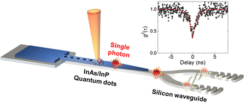
Scalable quantum photonic systems require efficient single photon sources coupled to integrated photonic devices. Solid-state quantum emitters can generate single photons with high efficiency, while silicon photonic circuits can manipulate them in an integrated device structure. Combining these two material platforms could, therefore, significantly increase the complexity of integrated quantum photonic devices. Here, we demonstrate hybrid integration of solid-state quantum emitters to a silicon photonic device. We develop a pick-and-place technique that can position epitaxially grown InAs/InP quantum dots emitting at telecom wavelengths on a silicon photonic chip deterministically with nanoscale precision. We employ an adiabatic tapering approach to transfer the emission from the quantum dots to the waveguide with high efficiency. We also incorporate an on-chip silicon-photonic beamsplitter to perform a Hanbury-Brown and Twiss measurement. Our approach could enable integration of precharacterized III–V quantum photonic devices into large-scale photonic structures to enable complex devices composed of many emitters and photons.
中文翻译:

固态量子发射器在硅光子芯片上的混合集成
可扩展的量子光子系统需要耦合到集成光子设备的高效单光子源。固态量子发射器可以高效地产生单个光子,而硅光子电路可以在集成的器件结构中操纵它们。因此,将这两种材料平台结合起来可能会大大增加集成量子光子器件的复杂性。在这里,我们演示了固态量子发射器与硅光子器件的混合集成。我们开发了一种拾放技术,可以以纳米级的精度确定性地将在电信波长发射的外延生长的InAs / InP量子点定位在硅光子芯片上。我们采用了一种绝热渐缩方法,以将发射效率从量子点转移到波导。我们还集成了片上硅光子分束器,以进行Hanbury-Brown和Twiss测量。我们的方法可以使预先表征的III–V量子光子器件集成到大规模光子结构中,从而实现由许多发射器和光子组成的复杂器件。
更新日期:2017-11-19
中文翻译:
固态量子发射器在硅光子芯片上的混合集成
可扩展的量子光子系统需要耦合到集成光子设备的高效单光子源。固态量子发射器可以高效地产生单个光子,而硅光子电路可以在集成的器件结构中操纵它们。因此,将这两种材料平台结合起来可能会大大增加集成量子光子器件的复杂性。在这里,我们演示了固态量子发射器与硅光子器件的混合集成。我们开发了一种拾放技术,可以以纳米级的精度确定性地将在电信波长发射的外延生长的InAs / InP量子点定位在硅光子芯片上。我们采用了一种绝热渐缩方法,以将发射效率从量子点转移到波导。我们还集成了片上硅光子分束器,以进行Hanbury-Brown和Twiss测量。我们的方法可以使预先表征的III–V量子光子器件集成到大规模光子结构中,从而实现由许多发射器和光子组成的复杂器件。


 京公网安备 11010802027423号