当前位置:
X-MOL 学术
›
ACS Photonics
›
论文详情
Our official English website, www.x-mol.net, welcomes your feedback! (Note: you will need to create a separate account there.)
Near-IR Imaging Based on Hot Carrier Generation in Nanometer-Scale Optical Coatings
ACS Photonics ( IF 7 ) Pub Date : 2017-11-10 00:00:00 , DOI: 10.1021/acsphotonics.7b01021 Lisa J. Krayer 1 , Elizabeth M. Tennyson 1 , Marina S. Leite 1 , Jeremy N. Munday 1
ACS Photonics ( IF 7 ) Pub Date : 2017-11-10 00:00:00 , DOI: 10.1021/acsphotonics.7b01021 Lisa J. Krayer 1 , Elizabeth M. Tennyson 1 , Marina S. Leite 1 , Jeremy N. Munday 1
Affiliation
|
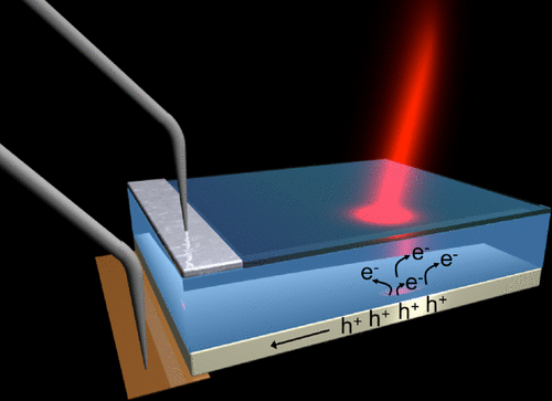
Silicon is the most widely used material for visible photodetection, with extensive applications in both consumer and industrial products. Further, its excellent optoelectronic properties and natural abundance have made it nearly ideal for microelectronic devices and solar cells. However, its lack of absorption in the infrared precludes its use in infrared detectors and imaging sensors, severely constraining its implementation in telecommunications. Here we show that this limitation can be overcome by exploiting resonant absorption in ultrathin metal films (<20 nm). Through appropriate optical design, a zeroth-order Fabry–Perot resonance is achieved, enabling ∼80% light absorption below the bandgap of the semiconductor. Absorption within the metal film results in excitation and injection of hot carriers through a Schottky junction into the Si. We experimentally demonstrate this phenomenon with four ultrathin planar metal films (Pt, Fe, Cr, and Ti), chosen to satisfy the resonant condition over a wide range of wavelengths (1200–1600 nm), and realize a near-infrared imaging detector. Our approach paves the way to implement a scalable, lithography free, and low-cost route to obtain silicon-based optoelectronics beyond the material bandgap.
中文翻译:

基于热载流子的纳米级光学镀膜近红外成像
硅是用于可见光检测的最广泛使用的材料,在消费和工业产品中都有广泛的应用。此外,其出色的光电性能和自然丰度使其几乎成为微电子设备和太阳能电池的理想选择。但是,由于其在红外光中缺乏吸收,因此无法在红外检测器和成像传感器中使用,从而严重限制了其在电信领域的应用。在这里,我们表明可以通过利用超薄金属膜(<20 nm)中的共振吸收来克服这一局限性。通过适当的光学设计,可以实现零级Fabry-Perot共振,从而在半导体的带隙以下实现约80%的光吸收。金属膜内的吸收导致激发热载流子,并通过肖特基结将热载流子注入到Si中。我们用四个超薄平面金属膜(Pt,Fe,Cr和Ti)证明了这种现象,选择它们来满足宽波长范围(1200-1600 nm)的共振条件,并实现了近红外成像检测器。我们的方法为实现可扩展,无光刻且低成本的途径铺平了道路,从而获得了材料带隙之外的基于硅的光电产品。
更新日期:2017-11-11
中文翻译:
基于热载流子的纳米级光学镀膜近红外成像
硅是用于可见光检测的最广泛使用的材料,在消费和工业产品中都有广泛的应用。此外,其出色的光电性能和自然丰度使其几乎成为微电子设备和太阳能电池的理想选择。但是,由于其在红外光中缺乏吸收,因此无法在红外检测器和成像传感器中使用,从而严重限制了其在电信领域的应用。在这里,我们表明可以通过利用超薄金属膜(<20 nm)中的共振吸收来克服这一局限性。通过适当的光学设计,可以实现零级Fabry-Perot共振,从而在半导体的带隙以下实现约80%的光吸收。金属膜内的吸收导致激发热载流子,并通过肖特基结将热载流子注入到Si中。我们用四个超薄平面金属膜(Pt,Fe,Cr和Ti)证明了这种现象,选择它们来满足宽波长范围(1200-1600 nm)的共振条件,并实现了近红外成像检测器。我们的方法为实现可扩展,无光刻且低成本的途径铺平了道路,从而获得了材料带隙之外的基于硅的光电产品。


 京公网安备 11010802027423号