Organic Electronics ( IF 3.2 ) Pub Date : 2017-11-05 , DOI: 10.1016/j.orgel.2017.10.031 Guoqiang Han , Xiumei Wang , Jun Zhang , Guocheng Zhang , Huihuang Yang , Daobin Hu , Dawei Sun , Xiaomin Wu , Yun Ye , Huipeng Chen , Tailiang Guo
|
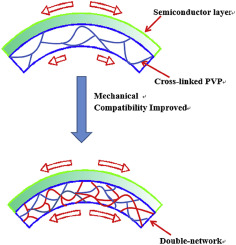
Taking inspiration from the characteristics and the limitations of flexible organic thin-film transistor (OTFT) devices, a novel surface modification method was proposed to modify the gate insulator to tune the mechanical compatibility and adhesion energy between gate insulator and semiconductor layer for high performance flexible OTFT devices. The surface modification method aimed to form a polymer network structure within the cross-linked polymer film by photo-polymerization of the liquid monomers which were infused into the cross-linked polymer film. The formation of double-network structure significantly improved the electrical performance of the flexible devices. The charge mobility increased from 0.17 cm2V−1s−1 to 1.52 cm2V−1s−1 and on/off current ratio increased by one or two orders of magnitude. During the bending tests, the devices modified with double-network dielectric structure exhibited excellent mechanical stability even after hundreds of successive bending cycles along with different bending radius. For instance, the mobility of the devices modified with methyl methacrylate only reduced by 2% after 500 successive bending cycles with a bending radius of 10 mm. It is ascribed to the improvement of mechanical compatibility and decrease of adhesion energy between gate insulator and semiconductor with the double network dielectric structure. More importantly, this work is a unique example to demonstrate the importance of mechanical compatibility and adhesion energy between gate insulator and semiconductor on the mechanical stability of flexible OTFT. Furthermore, these results clearly demonstrated that this method is a promising tool to tune the semiconductor/dielectric interface, especially the mechanical compatibility and adhesion energy between semiconductor layer and dielectric layer, which has great potential for high performance flexible OTFTs with excellent mechanical stability.
中文翻译:
具有双网络介电结构的接口工程,用于柔性有机薄膜晶体管
从柔性有机薄膜晶体管(OTFT)器件的特性和局限性中获得启发,提出了一种新的表面改性方法来改性栅绝缘体,以调节栅绝缘体与半导体层之间的机械相容性和粘附能,从而获得高性能的柔性OTFT器件。该表面改性方法旨在通过使注入到交联的聚合物膜中的液体单体进行光聚合来在交联的聚合物膜中形成聚合物网络结构。双网状结构的形成显着改善了柔性装置的电气性能。电荷迁移率从0.17 cm 2 V -1 s -1增加到1.52 cm 2 V-1秒-1开/关电流比增加了一个或两个数量级。在弯曲测试期间,即使经过数百次连续弯曲循环以及不同的弯曲半径,采用双网状介电结构改性的器件仍具有出色的机械稳定性。例如,用甲基丙烯酸甲酯改性的器件的迁移率在连续10次弯曲半径为10 mm的弯曲循环后仅降低了2%。这归因于具有双网络介电结构的机械相容性的提高和栅极绝缘体与半导体之间的粘附能的降低。更重要的是,这项工作是一个独特的例子,展示了机械兼容性和栅极绝缘体与半导体之间的粘附能对柔性OTFT的机械稳定性的重要性。此外,


 京公网安备 11010802027423号