Organic Electronics ( IF 3.2 ) Pub Date : 2017-10-28 , DOI: 10.1016/j.orgel.2017.10.036 Min Su Kim , Dong-Hoon Lee , Hyeong Jun Cho , Jongsu Oh , So Young Lee , Jae Moon Kim , KeeChan Park , Yong-Sang Kim
|
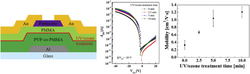
We investigated the indirect UV/ozone treatment, which means treating the insulator surface under tens of nanometers, rather than the direct surface of the insulator. The double-stacked organic layers are used as gate insulator and the UV/ozone treatment is conducted between these two layers. We analyzed the surface morphologies of the gate insulator and the pentacene by atomic force microscopy (AFM) to confirm the effect of indirect UV/ozone treatment. The UV/ozone treatment reduced the surface roughness of the upper side gate insulator and increased the pentacene grain size. Pentacene-based thin film transistors were fabricated and the electrical property improvement after this treatment was examined. The largest improvement was found when the UV/ozone treatment time is 10 min and the upper side gate insulator thickness is 20 nm, and the mobility at that condition is 1.21 cm2/V s, which is larger than three times that without UV/ozone treatment (0.33 cm2/V s).
中文翻译:
间接紫外线/臭氧处理对具有双堆叠有机栅极绝缘体的并五苯薄膜晶体管的影响
我们研究了间接UV /臭氧处理,这意味着在几十纳米以下处理绝缘子表面,而不是在绝缘子的直接表面上进行处理。将双层有机层用作栅极绝缘体,并在这两层之间进行UV /臭氧处理。我们通过原子力显微镜(AFM)分析了栅极绝缘体和并五苯的表面形态,以确认间接UV /臭氧处理的效果。UV /臭氧处理降低了上侧栅极绝缘体的表面粗糙度,并增加了并五苯的晶粒尺寸。制造了并五苯系薄膜晶体管,并研究了该处理后的电性能改善。当紫外线/臭氧处理时间为10分钟且上侧栅极绝缘体厚度为20 nm时,发现最大的改进,2 / V s,是未进行紫外线/臭氧处理的三倍(0.33 cm 2 / V s)。


 京公网安备 11010802027423号