当前位置:
X-MOL 学术
›
ACS Appl. Mater. Interfaces
›
论文详情
Our official English website, www.x-mol.net, welcomes your feedback! (Note: you will need to create a separate account there.)
High-Efficiency InGaN/GaN Quantum Well-Based Vertical Light-Emitting Diodes Fabricated on β-Ga2O3 Substrate
ACS Applied Materials & Interfaces ( IF 9.5 ) Pub Date : 2017-09-22 00:00:00 , DOI: 10.1021/acsami.7b09584 Mufasila M. Muhammed 1 , Norah Alwadai 1 , Sergei Lopatin 2 , Akito Kuramata 3 , Iman S. Roqan 1
ACS Applied Materials & Interfaces ( IF 9.5 ) Pub Date : 2017-09-22 00:00:00 , DOI: 10.1021/acsami.7b09584 Mufasila M. Muhammed 1 , Norah Alwadai 1 , Sergei Lopatin 2 , Akito Kuramata 3 , Iman S. Roqan 1
Affiliation
|
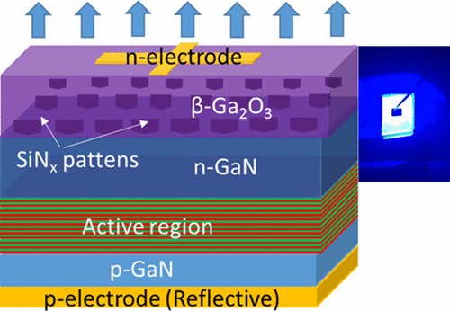
We demonstrate a state-of-the-art high-efficiency GaN-based vertical light-emitting diode (VLED) grown on a transparent and conductive (−201)-oriented (β-Ga2O3) substrate, obtained using a straightforward growth process that does not require a high-cost lift-off technique or complex fabrication process. The high-resolution scanning transmission electron microscopy (STEM) images confirm that we produced high quality upper layers, including a multiquantum well (MQW) grown on the masked β-Ga2O3 substrate. STEM imaging also shows a well-defined MQW without InN diffusion into the barrier. Electroluminescence (EL) measurements at room temperature indicate that we achieved a very high internal quantum efficiency (IQE) of 78%; at lower temperatures, IQE reaches ∼86%. The photoluminescence (PL) and time-resolved PL analysis indicate that, at a high carrier injection density, the emission is dominated by radiative recombination with a negligible Auger effect; no quantum-confined Stark effect is observed. At low temperatures, no efficiency droop is observed at a high carrier injection density, indicating the superior VLED structure obtained without lift-off processing, which is cost-effective for large-scale devices.
中文翻译:

高效率的InGaN /氮化镓量子阱基于垂直发光二极管上制造的β-Ga 2 ö 3基板
我们证明生长在透明且导电的(-201)的基于氮化镓的国家的最先进的高效率垂直发光二极管(VLED)取向的(的β-Ga 2 ö 3)衬底,使用一个简单的获得不需要高成本的剥离技术或复杂的制造过程的生长过程。高分辨率扫描透射电子显微镜(STEM)图像证实,我们产生生长在掩蔽高质量上层,包括多量子阱(MQW)的β-Ga 2 ö 3基质。STEM成像还显示出清晰的MQW,而InN不会扩散到势垒中。室温下的电致发光(EL)测量表明,我们实现了78%的非常高的内部量子效率(IQE)。在较低温度下,IQE达到约86%。光致发光(PL)和时间分辨的PL分析表明,在高载流子注入密度下,发射主要由辐射复合引起,而俄歇效应可忽略不计。没有观察到量子限制的斯塔克效应。在低温下,在高载流子注入密度下未观察到效率下降,这表明无需剥离工艺即可获得优异的VLED结构,这对于大规模器件而言具有成本效益。
更新日期:2017-09-22
中文翻译:
高效率的InGaN /氮化镓量子阱基于垂直发光二极管上制造的β-Ga 2 ö 3基板
我们证明生长在透明且导电的(-201)的基于氮化镓的国家的最先进的高效率垂直发光二极管(VLED)取向的(的β-Ga 2 ö 3)衬底,使用一个简单的获得不需要高成本的剥离技术或复杂的制造过程的生长过程。高分辨率扫描透射电子显微镜(STEM)图像证实,我们产生生长在掩蔽高质量上层,包括多量子阱(MQW)的β-Ga 2 ö 3基质。STEM成像还显示出清晰的MQW,而InN不会扩散到势垒中。室温下的电致发光(EL)测量表明,我们实现了78%的非常高的内部量子效率(IQE)。在较低温度下,IQE达到约86%。光致发光(PL)和时间分辨的PL分析表明,在高载流子注入密度下,发射主要由辐射复合引起,而俄歇效应可忽略不计。没有观察到量子限制的斯塔克效应。在低温下,在高载流子注入密度下未观察到效率下降,这表明无需剥离工艺即可获得优异的VLED结构,这对于大规模器件而言具有成本效益。


 京公网安备 11010802027423号