当前位置:
X-MOL 学术
›
ACS Appl. Mater. Interfaces
›
论文详情
Our official English website, www.x-mol.net, welcomes your feedback! (Note: you will need to create a separate account there.)
Polarization-Dependent Photoinduced Bias-Stress Effect in Single-Crystal Organic Field-Effect Transistors
ACS Applied Materials & Interfaces ( IF 9.5 ) Pub Date : 2017-09-21 00:00:00 , DOI: 10.1021/acsami.7b11134 Hyun Ho Choi 1 , Hikmet Najafov , Nikolai Kharlamov 2 , Denis V. Kuznetsov 2 , Sergei I. Didenko 2 , Kilwon Cho 1 , Alejandro L. Briseno 3 , Vitaly Podzorov 2
ACS Applied Materials & Interfaces ( IF 9.5 ) Pub Date : 2017-09-21 00:00:00 , DOI: 10.1021/acsami.7b11134 Hyun Ho Choi 1 , Hikmet Najafov , Nikolai Kharlamov 2 , Denis V. Kuznetsov 2 , Sergei I. Didenko 2 , Kilwon Cho 1 , Alejandro L. Briseno 3 , Vitaly Podzorov 2
Affiliation
|
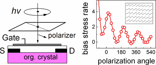
Photoinduced charge transfer between semiconductors and gate dielectrics can occur in organic field-effect transistors (OFETs) operating under illumination, leading to a pronounced bias-stress effect in devices that are normally stable while operating in the dark. Here, we report an observation of a polarization-dependent photoinduced bias-stress effect in two prototypical single-crystal OFETs, based on rubrene and tetraphenylbis(indolo{1,2-a})quinolin. We find that the decay rate of the source–drain current in these OFETs under illumination is a periodic function of the polarization angle of incident photoexcitation with respect to the crystal axes, with a periodicity of π. The angular positions of maxima and minima of the bias-stress rate match those of the optical absorption coefficient of the corresponding crystals. The analysis of the effect shows that it stems from a charge transfer of “hot” holes, photogenerated in the crystal within a very short thermalization length (≪μm) from the semiconductor–dielectric interface. The observed phenomenon is a type of intrinsic structure–property relationship, revealing how molecular packing affects parameter drift in organic transistors under illumination. We also demonstrate that a photoinduced charge transfer in OFETs can be used for recording rewritable accumulation channels with an optically defined geometry and resolution, which can be used in a number of potential applications.
中文翻译:

单晶有机场效应晶体管中偏振相关的光致偏压效应。
半导体和栅极电介质之间的光感应电荷转移可能发生在在光照下工作的有机场效应晶体管(OFET)中,从而导致通常在黑暗中工作时仍保持稳定的器件产生明显的偏置应力效应。在这里,我们报告了基于红rub烯和四苯基双(indolo {1,2- a})喹啉。我们发现,在光照下这些OFET中的源极-漏极电流的衰减率是入射光激发的偏振角相对于晶轴的周期性函数,其周期性为π。偏应力率的最大值和最小值的角位置与相应晶体的光吸收系数的角位置匹配。对该效应的分析表明,其源于“热”空穴的电荷转移,该空穴在距半导体-介电界面很短的热化长度(≪μm)内在晶体中光生。观察到的现象是一种内在的结构与属性的关系,揭示了分子堆积如何在光照下影响有机晶体管中的参数漂移。
更新日期:2017-09-21
中文翻译:
单晶有机场效应晶体管中偏振相关的光致偏压效应。
半导体和栅极电介质之间的光感应电荷转移可能发生在在光照下工作的有机场效应晶体管(OFET)中,从而导致通常在黑暗中工作时仍保持稳定的器件产生明显的偏置应力效应。在这里,我们报告了基于红rub烯和四苯基双(indolo {1,2- a})喹啉。我们发现,在光照下这些OFET中的源极-漏极电流的衰减率是入射光激发的偏振角相对于晶轴的周期性函数,其周期性为π。偏应力率的最大值和最小值的角位置与相应晶体的光吸收系数的角位置匹配。对该效应的分析表明,其源于“热”空穴的电荷转移,该空穴在距半导体-介电界面很短的热化长度(≪μm)内在晶体中光生。观察到的现象是一种内在的结构与属性的关系,揭示了分子堆积如何在光照下影响有机晶体管中的参数漂移。


 京公网安备 11010802027423号