Our official English website, www.x-mol.net, welcomes your feedback! (Note: you will need to create a separate account there.)
On‐Chip: Direct Microrolling Processing on a Silicon Wafer (Small 36/2017)
Small ( IF 13.3 ) Pub Date : 2017-09-21 , DOI: 10.1002/smll.201770195 Kanna Aoki 1 , Keita Ishiguro 1 , Masaki Denokami 1 , Yuya Tanahashi 1 , Kentaro Furusawa 2 , Norihiko Sekine 2 , Tadafumi Adschiri 3 , Minoru Fujii 1
Small ( IF 13.3 ) Pub Date : 2017-09-21 , DOI: 10.1002/smll.201770195 Kanna Aoki 1 , Keita Ishiguro 1 , Masaki Denokami 1 , Yuya Tanahashi 1 , Kentaro Furusawa 2 , Norihiko Sekine 2 , Tadafumi Adschiri 3 , Minoru Fujii 1
Affiliation
|
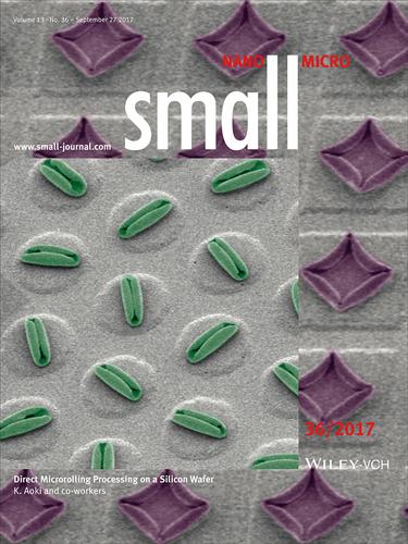
In article number 1701630, Kanna Aoki and co‐workers achieve patterning of porosified silicon wafer surfaces using anodic oxidation, and conventional photolithography and wet etching. Subsequent oxidation treatment facilitated self‐rolling in the porous silicon layers. Various three‐dimensional shapes such as bowls, tubes, and boxes were realized. A direct silicon‐processing technology that enables thin layers of silicon surfaces to be bent into various three‐dimensional curved structures at the micron scale is useful for expanding the capabilities and design possibilities of on‐chip Si devices.

中文翻译:

芯片上:在硅晶圆上进行直接微轧加工(Small 36/2017)
在编号1701630中,Kanna Aoki及其同事使用阳极氧化,常规光刻和湿法蚀刻技术对多孔硅晶片表面进行了图案化。随后的氧化处理促进了多孔硅层中的自滚动。实现了各种三维形状,例如碗,管子和盒子。一种直接的硅加工技术,可使硅表面的薄层以微米级弯曲成各种三维弯曲结构,对于扩展片上硅器件的功能和设计可能性非常有用。
更新日期:2017-09-21
中文翻译:
芯片上:在硅晶圆上进行直接微轧加工(Small 36/2017)
在编号1701630中,Kanna Aoki及其同事使用阳极氧化,常规光刻和湿法蚀刻技术对多孔硅晶片表面进行了图案化。随后的氧化处理促进了多孔硅层中的自滚动。实现了各种三维形状,例如碗,管子和盒子。一种直接的硅加工技术,可使硅表面的薄层以微米级弯曲成各种三维弯曲结构,对于扩展片上硅器件的功能和设计可能性非常有用。


 京公网安备 11010802027423号