Our official English website, www.x-mol.net, welcomes your feedback! (Note: you will need to create a separate account there.)
van der Waals epitaxial two-dimensional CdSxSe(1−x) semiconductor alloys with tunable-composition and application to flexible optoelectronics
Nanoscale ( IF 6.7 ) Pub Date : 2017-08-04 00:00:00 , DOI: 10.1039/c7nr04968d Jing Xia 1, 2, 3, 4, 5 , Yun-Xuan Zhao 1, 2, 3, 4, 5 , Lei Wang 1, 2, 3, 4, 5 , Xuan-Ze Li 1, 2, 3, 4, 5 , Yi-Yi Gu 1, 2, 3, 4, 5 , Hua-Qiu Cheng 1, 2, 3, 4, 5 , Xiang-Min Meng 1, 2, 3, 4, 5
Nanoscale ( IF 6.7 ) Pub Date : 2017-08-04 00:00:00 , DOI: 10.1039/c7nr04968d Jing Xia 1, 2, 3, 4, 5 , Yun-Xuan Zhao 1, 2, 3, 4, 5 , Lei Wang 1, 2, 3, 4, 5 , Xuan-Ze Li 1, 2, 3, 4, 5 , Yi-Yi Gu 1, 2, 3, 4, 5 , Hua-Qiu Cheng 1, 2, 3, 4, 5 , Xiang-Min Meng 1, 2, 3, 4, 5
Affiliation
|
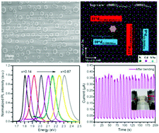
Despite the substantial progress in the development of two-dimensional (2D) materials from conventional layered crystals, it still remains particularly challenging to produce high-quality 2D non-layered semiconductor alloys which may bring in some unique properties and new functions. In this work, the synthesis of well-oriented 2D non-layered CdSxSe(1−x) semiconductor alloy flakes with tunable compositions and optical properties is established. Structural analysis reveals that the 2D non-layered alloys follow an incommensurate van der Waals epitaxial growth pattern. Photoluminescence measurements show that the 2D alloys have composition-dependent direct bandgaps with the emission peak varying from 1.8 eV to 2.3 eV, coinciding well with the density functional theory calculations. Furthermore, photodetectors based on the CdSxSe(1−x) flakes exhibit a high photoresponsivity of 703 A W−1 with an external quantum efficiency of 1.94 × 10³ and a response time of 39 ms. Flexible devices fabricated on a thin mica substrate display good mechanical stability upon repeated bending. This work suggests a facile and general method to produce high-quality 2D non-layered semiconductor alloys for next-generation optoelectronic devices.
中文翻译:

具有可调成分的范德华外延二维CdS x Se (1- x)半导体合金及其在柔性光电中的应用
尽管从常规层状晶体开发二维(2D)材料方面取得了重大进展,但生产高质量的二维非层状半导体合金仍然可能特别具有挑战性,这种合金可能会带来一些独特的性能和新功能。在这项工作中,定向良好的2D非分层CdS x Se (1- x)的合成建立了具有可调组成和光学特性的半导体合金薄片。结构分析表明,二维非层状合金遵循不相称的范德华斯外延生长模式。光致发光测量表明,二维合金具有与组成有关的直接带隙,其发射峰在1.8 eV至2.3 eV之间变化,与密度泛函理论计算非常吻合。此外,基于CdS x Se (1- x)薄片的光电探测器表现出703 AW -1的高光响应性,外部量子效率为1.94×10 3响应时间为39毫秒。在薄云母基板上制造的柔性器件在反复弯曲时显示出良好的机械稳定性。这项工作提出了一种简便而通用的方法来生产用于下一代光电器件的高质量2D非层状半导体合金。
更新日期:2017-09-21
中文翻译:
具有可调成分的范德华外延二维CdS x Se (1- x)半导体合金及其在柔性光电中的应用
尽管从常规层状晶体开发二维(2D)材料方面取得了重大进展,但生产高质量的二维非层状半导体合金仍然可能特别具有挑战性,这种合金可能会带来一些独特的性能和新功能。在这项工作中,定向良好的2D非分层CdS x Se (1- x)的合成建立了具有可调组成和光学特性的半导体合金薄片。结构分析表明,二维非层状合金遵循不相称的范德华斯外延生长模式。光致发光测量表明,二维合金具有与组成有关的直接带隙,其发射峰在1.8 eV至2.3 eV之间变化,与密度泛函理论计算非常吻合。此外,基于CdS x Se (1- x)薄片的光电探测器表现出703 AW -1的高光响应性,外部量子效率为1.94×10 3响应时间为39毫秒。在薄云母基板上制造的柔性器件在反复弯曲时显示出良好的机械稳定性。这项工作提出了一种简便而通用的方法来生产用于下一代光电器件的高质量2D非层状半导体合金。


 京公网安备 11010802027423号