当前位置:
X-MOL 学术
›
Nano Lett.
›
论文详情
Our official English website, www.x-mol.net, welcomes your feedback! (Note: you will need to create a separate account there.)
Improving the Performance of Graphene Phototransistors Using a Heterostructure as the Light-Absorbing Layer
Nano Letters ( IF 10.8 ) Pub Date : 2017-09-14 00:00:00 , DOI: 10.1021/acs.nanolett.7b03263 Xiaoqing Chen 1, 2 , Xiaolong Liu 1, 3 , Bing Wu 1 , Haiyan Nan 4 , Hui Guo 2 , Zhenhua Ni 4 , Fengqiu Wang 1 , Xiaomu Wang 1 , Yi Shi 1 , Xinran Wang 1
Nano Letters ( IF 10.8 ) Pub Date : 2017-09-14 00:00:00 , DOI: 10.1021/acs.nanolett.7b03263 Xiaoqing Chen 1, 2 , Xiaolong Liu 1, 3 , Bing Wu 1 , Haiyan Nan 4 , Hui Guo 2 , Zhenhua Ni 4 , Fengqiu Wang 1 , Xiaomu Wang 1 , Yi Shi 1 , Xinran Wang 1
Affiliation
|
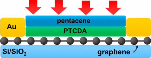
Interfacing light-sensitive semiconductors with graphene can afford high-gain phototransistors by the multiplication effect of carriers in the semiconductor layer. So far, most devices consist of one semiconductor light-absorbing layer, where the lack of internal built-in field can strongly reduce the quantum efficiency and bandwidth. Here, we demonstrate a much improved graphene phototransistor performances using an epitaxial organic heterostructure composed of perylene-3,4,9,10-tetracarboxylic dianhydride (PTCDA) and pentacene as the light-absorbing layer. Compared with single light-absorbing material, the responsivity and response time can be simultaneously improved by 1 and 2 orders of magnitude over a broad band of 400–700 nm, under otherwise the same experimental conditions. As a result, the external quantum efficiency increases by over 800 times. Furthermore, the response time of the heterostructured phototransistor is highly gate-tunable down to sub-30 μs, which is among the fastest in the sensitized graphene phototransistors interfacing with electrically passive light-absorbing semiconductors. We show that the improvement is dominated by the efficient electron–hole pair dissociation due to interfacial built-in field rather than bulk absorption. The structure demonstrated here can be extended to many other organic and inorganic semiconductors, which opens new possibilities for high-performance graphene-based optoelectronics.
中文翻译:

使用异质结构作为光吸收层改善石墨烯光电晶体管的性能
通过半导体层中载流子的倍增效应,光敏半导体与石墨烯的接口可以提供高增益的光电晶体管。到目前为止,大多数设备都由一个半导体光吸收层组成,其中缺乏内部内置电场会极大地降低量子效率和带宽。在这里,我们证明了使用由per 3,4,9,10-四羧酸二酐(PTCDA)和并五苯组成的外延有机异质结构作为光吸收层,可以大大改善石墨烯光电晶体管的性能。与单一吸光材料相比,在其他实验条件相同的情况下,在400-700 nm的宽带范围内,响应度和响应时间可以同时提高1和2个数量级。因此,外部量子效率提高了800倍以上。此外,异质结构光电晶体管的响应时间可在低至30μs的范围内高度可调,这在与电学无源光吸收半导体接口的敏化石墨烯光电晶体管中是最快的。我们表明,这种改善主要归因于界面内置场而不是整体吸收引起的有效的电子-空穴对解离。此处演示的结构可以扩展到许多其他有机和无机半导体,这为高性能基于石墨烯的光电子学打开了新的可能性。在与无源光吸收半导体接口的敏化石墨烯光电晶体管中,它是最快的。我们表明,这种改善主要归因于界面内置场而不是整体吸收引起的有效的电子-空穴对解离。此处演示的结构可以扩展到许多其他有机和无机半导体,这为高性能基于石墨烯的光电子学打开了新的可能性。在与无源光吸收半导体接口的敏化石墨烯光电晶体管中,它是最快的。我们表明,这种改善主要归因于界面内置场而不是整体吸收引起的有效的电子-空穴对解离。此处演示的结构可以扩展到许多其他有机和无机半导体,这为高性能基于石墨烯的光电子学打开了新的可能性。
更新日期:2017-09-15
中文翻译:
使用异质结构作为光吸收层改善石墨烯光电晶体管的性能
通过半导体层中载流子的倍增效应,光敏半导体与石墨烯的接口可以提供高增益的光电晶体管。到目前为止,大多数设备都由一个半导体光吸收层组成,其中缺乏内部内置电场会极大地降低量子效率和带宽。在这里,我们证明了使用由per 3,4,9,10-四羧酸二酐(PTCDA)和并五苯组成的外延有机异质结构作为光吸收层,可以大大改善石墨烯光电晶体管的性能。与单一吸光材料相比,在其他实验条件相同的情况下,在400-700 nm的宽带范围内,响应度和响应时间可以同时提高1和2个数量级。因此,外部量子效率提高了800倍以上。此外,异质结构光电晶体管的响应时间可在低至30μs的范围内高度可调,这在与电学无源光吸收半导体接口的敏化石墨烯光电晶体管中是最快的。我们表明,这种改善主要归因于界面内置场而不是整体吸收引起的有效的电子-空穴对解离。此处演示的结构可以扩展到许多其他有机和无机半导体,这为高性能基于石墨烯的光电子学打开了新的可能性。在与无源光吸收半导体接口的敏化石墨烯光电晶体管中,它是最快的。我们表明,这种改善主要归因于界面内置场而不是整体吸收引起的有效的电子-空穴对解离。此处演示的结构可以扩展到许多其他有机和无机半导体,这为高性能基于石墨烯的光电子学打开了新的可能性。在与无源光吸收半导体接口的敏化石墨烯光电晶体管中,它是最快的。我们表明,这种改善主要归因于界面内置场而不是整体吸收引起的有效的电子-空穴对解离。此处演示的结构可以扩展到许多其他有机和无机半导体,这为高性能基于石墨烯的光电子学打开了新的可能性。


 京公网安备 11010802027423号