当前位置:
X-MOL 学术
›
J. Mater. Chem. C
›
论文详情
Our official English website, www.x-mol.net, welcomes your feedback! (Note: you will need to create a separate account there.)
Single quantum dot rectifying diode with tunable threshold voltage
Journal of Materials Chemistry C ( IF 6.4 ) Pub Date : 2017-08-30 00:00:00 , DOI: 10.1039/c7tc02537h Gopal S. Kenath 1, 2, 3, 4 , Piyali Maity 3, 4, 5, 6 , Yogesh Kumar 2, 3, 4, 7 , Hemant Kumar 2, 3, 4, 7 , Vinod K. Gangwar 2, 3, 4, 5 , Sandip Chaterjee 2, 3, 4, 5 , Satyabrata Jit 2, 3, 4, 7 , Anup K. Ghosh 3, 4, 5, 6 , Bhola N. Pal 1, 2, 3, 4
Journal of Materials Chemistry C ( IF 6.4 ) Pub Date : 2017-08-30 00:00:00 , DOI: 10.1039/c7tc02537h Gopal S. Kenath 1, 2, 3, 4 , Piyali Maity 3, 4, 5, 6 , Yogesh Kumar 2, 3, 4, 7 , Hemant Kumar 2, 3, 4, 7 , Vinod K. Gangwar 2, 3, 4, 5 , Sandip Chaterjee 2, 3, 4, 5 , Satyabrata Jit 2, 3, 4, 7 , Anup K. Ghosh 3, 4, 5, 6 , Bhola N. Pal 1, 2, 3, 4
Affiliation
|
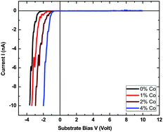
An ambient atmosphere single quantum dot (QDs) rectifying diode with tunable threshold voltage has been fabricated using cobalt (Co) doped CdS QDs with a device structure of ITO/ZnO/QDs. Current–voltage (I–V) characterization of this device has been tested using ambient atmosphere scanning tunnelling microscope (STM). The scanning tunnelling spectra (STS) shows a very high rectification behavior of this single dot based device with a ratio of 103. The threshold voltage of this device decreases with increase in doping concentration of QDs. Reduction of this turn-on voltage occurs due to the formation of additional energy band of Co impurity within the band gap of QDs that exist closer to the valance band (VB) of CdS. Existence of this additional energy band has also been observed in the UV-VIS absorption data of Co doped CdS, which introduces an additional absorption peak in the near infrared region. This impurity band is fully populated at room temperature and the width of this band increases with doping concentration, which is the key for the tunability of threshold voltage. This finding has been explained with one empirical model of relative band shifting of semiconductor–QDs–tip interfaces with positive and negative substrate bias.
中文翻译:

具有可调阈值电压的单量子点整流二极管
使用具有ITO / ZnO / QDs器件结构的掺钴(Cd)的CdS QD,制造了具有可调阈值电压的环境大气单量子点(QDs)整流二极管。电流-电压(我- V)本装置的特征已使用环境气氛扫描隧道显微镜(STM)的测试。扫描隧道光谱(STS)显示该单点器件的整流性能非常高,比率为10 3。该器件的阈值电压随着QD掺杂浓度的增加而降低。导通电压的降低是由于在QD的带隙内形成了Co杂质的附加能带所致,这些带隙更靠近CdS的价带(VB)。在掺Co的CdS的UV-VIS吸收数据中也观察到了该附加能带的存在,这在近红外区域引入了附加吸收峰。该杂质带在室温下完全填充,并且该带的宽度随掺杂浓度而增加,这是阈值电压可调性的关键。这一发现已经用一种具有正负衬底偏置的半导体-QDs-尖端界面的相对带移的经验模型进行了解释。
更新日期:2017-09-15
中文翻译:
具有可调阈值电压的单量子点整流二极管
使用具有ITO / ZnO / QDs器件结构的掺钴(Cd)的CdS QD,制造了具有可调阈值电压的环境大气单量子点(QDs)整流二极管。电流-电压(我- V)本装置的特征已使用环境气氛扫描隧道显微镜(STM)的测试。扫描隧道光谱(STS)显示该单点器件的整流性能非常高,比率为10 3。该器件的阈值电压随着QD掺杂浓度的增加而降低。导通电压的降低是由于在QD的带隙内形成了Co杂质的附加能带所致,这些带隙更靠近CdS的价带(VB)。在掺Co的CdS的UV-VIS吸收数据中也观察到了该附加能带的存在,这在近红外区域引入了附加吸收峰。该杂质带在室温下完全填充,并且该带的宽度随掺杂浓度而增加,这是阈值电压可调性的关键。这一发现已经用一种具有正负衬底偏置的半导体-QDs-尖端界面的相对带移的经验模型进行了解释。


 京公网安备 11010802027423号