当前位置:
X-MOL 学术
›
Nano Lett.
›
论文详情
Our official English website, www.x-mol.net, welcomes your feedback! (Note: you will need to create a separate account there.)
Effective Surface Passivation of InP Nanowires by Atomic-Layer-Deposited Al2O3 with POx Interlayer
Nano Letters ( IF 10.8 ) Pub Date : 2017-09-11 00:00:00 , DOI: 10.1021/acs.nanolett.7b02972 L. E. Black 1 , A. Cavalli 1 , M. A. Verheijen 1, 2 , J. E. M. Haverkort 1 , E. P. A. M. Bakkers 1 , W. M. M. Kessels 1
Nano Letters ( IF 10.8 ) Pub Date : 2017-09-11 00:00:00 , DOI: 10.1021/acs.nanolett.7b02972 L. E. Black 1 , A. Cavalli 1 , M. A. Verheijen 1, 2 , J. E. M. Haverkort 1 , E. P. A. M. Bakkers 1 , W. M. M. Kessels 1
Affiliation
|
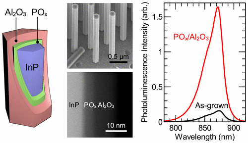
III/V semiconductor nanostructures have significant potential in device applications, but effective surface passivation is critical due to their large surface-to-volume ratio. For InP such passivation has proven particularly difficult, with substantial depassivation generally observed following dielectric deposition on InP surfaces. We present a novel approach based on passivation with a phosphorus-rich interfacial oxide deposited using a low-temperature process, which is critical to avoid P-desorption. For this purpose we have chosen a POx layer deposited in a plasma-assisted atomic layer deposition (ALD) system at room temperature. Since POx is known to be hygroscopic and therefore unstable in atmosphere, we encapsulate this layer with a thin ALD Al2O3 capping layer to form a POx/Al2O3 stack. This passivation scheme is capable of improving the photoluminescence (PL) efficiency of our state-of-the-art wurtzite (WZ) InP nanowires by a factor of ∼20 at low excitation. If we apply the rate equation analysis advocated by some authors, we derive a PL internal quantum efficiency (IQE) of 75% for our passivated wires at high excitation. Our results indicate that it is more reliable to calculate the IQE as the ratio of the integrated PL intensity at room temperature to that at 10 K. By this means we derive an IQE of 27% for the passivated wires at high excitation (>10 kW cm–2), which constitutes an unprecedented level of performance for undoped InP nanowires. This conclusion is supported by time-resolved PL decay lifetimes, which are also shown to be significantly higher than previously reported for similar wires. The passivation scheme displays excellent long-term stability (>7 months) and is additionally shown to substantially improve the thermal stability of InP surfaces (>300 °C), significantly expanding the temperature window for device processing. Such effective surface passivation is a key enabling technology for InP nanowire devices such as nanolasers and solar cells.
中文翻译:

带有PO x夹层的原子层沉积Al 2 O 3对InP纳米线进行有效的表面钝化
III / V半导体纳米结构在设备应用中具有巨大潜力,但有效的表面钝化因其大的表面体积比而至关重要。对于InP,这种钝化已被证明特别困难,在InP表面进行电介质沉积后,通常会观察到大量的钝化。我们提出了一种基于钝化工艺的新型方法,该工艺采用低温工艺沉积的富含磷的界面氧化物,这对于避免P脱附至关重要。为此,我们选择了在室温下在等离子体辅助原子层沉积(ALD)系统中沉积的PO x层。由于已知PO x具有吸湿性,因此在大气中不稳定,因此我们用薄的ALD Al封装该层2 O 3覆盖层形成PO x / Al 2 O 3叠层。这种钝化方案能够在低激发下将我们最新的纤锌矿(WZ)InP纳米线的光致发光(PL)效率提高约20倍。如果我们采用一些作者提倡的速率方程分析,我们得出的钝化线在高激发下的PL内部量子效率(IQE)为75%。我们的结果表明,将IQE计算为室温下与10 K下的PL积分强度之比是更可靠的。通过这种方法,我们得出在高励磁(> 10 kW)下钝化线的IQE为27%厘米–2),这构成了非掺杂InP纳米线前所未有的性能水平。时间分辨的PL衰减寿命支持了这一结论,该寿命也被证明比以前报道的类似导线要高得多。钝化方案具有出色的长期稳定性(> 7个月),另外还显示出可以显着改善InP表面的热稳定性(> 300°C),从而大大扩展了器件加工的温度范围。这种有效的表面钝化是InP纳米线器件(例如纳米激光器和太阳能电池)的关键启用技术。
更新日期:2017-09-12
中文翻译:
带有PO x夹层的原子层沉积Al 2 O 3对InP纳米线进行有效的表面钝化
III / V半导体纳米结构在设备应用中具有巨大潜力,但有效的表面钝化因其大的表面体积比而至关重要。对于InP,这种钝化已被证明特别困难,在InP表面进行电介质沉积后,通常会观察到大量的钝化。我们提出了一种基于钝化工艺的新型方法,该工艺采用低温工艺沉积的富含磷的界面氧化物,这对于避免P脱附至关重要。为此,我们选择了在室温下在等离子体辅助原子层沉积(ALD)系统中沉积的PO x层。由于已知PO x具有吸湿性,因此在大气中不稳定,因此我们用薄的ALD Al封装该层2 O 3覆盖层形成PO x / Al 2 O 3叠层。这种钝化方案能够在低激发下将我们最新的纤锌矿(WZ)InP纳米线的光致发光(PL)效率提高约20倍。如果我们采用一些作者提倡的速率方程分析,我们得出的钝化线在高激发下的PL内部量子效率(IQE)为75%。我们的结果表明,将IQE计算为室温下与10 K下的PL积分强度之比是更可靠的。通过这种方法,我们得出在高励磁(> 10 kW)下钝化线的IQE为27%厘米–2),这构成了非掺杂InP纳米线前所未有的性能水平。时间分辨的PL衰减寿命支持了这一结论,该寿命也被证明比以前报道的类似导线要高得多。钝化方案具有出色的长期稳定性(> 7个月),另外还显示出可以显着改善InP表面的热稳定性(> 300°C),从而大大扩展了器件加工的温度范围。这种有效的表面钝化是InP纳米线器件(例如纳米激光器和太阳能电池)的关键启用技术。


 京公网安备 11010802027423号