当前位置:
X-MOL 学术
›
Adv. Funct. Mater.
›
论文详情
Our official English website, www.x-mol.net, welcomes your feedback! (Note: you will need to create a separate account there.)
Large‐Area Chemical Vapor Deposited MoS2 with Transparent Conducting Oxide Contacts toward Fully Transparent 2D Electronics
Advanced Functional Materials ( IF 19.0 ) Pub Date : 2017-09-08 , DOI: 10.1002/adfm.201703119 Zhenyu Dai 1 , Zhenwei Wang 1 , Xin He 1 , Xi-Xiang Zhang 1 , Husam N. Alshareef 1
Advanced Functional Materials ( IF 19.0 ) Pub Date : 2017-09-08 , DOI: 10.1002/adfm.201703119 Zhenyu Dai 1 , Zhenwei Wang 1 , Xin He 1 , Xi-Xiang Zhang 1 , Husam N. Alshareef 1
Affiliation
|
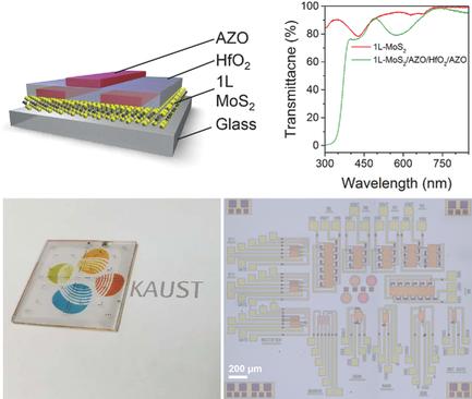
2D semiconductors are poised to revolutionize the future of electronics and photonics, much like transparent oxide conductors and semiconductors have revolutionized the display industry. Herein, these two types of materials are combined to realize fully transparent 2D electronic devices and circuits. Specifically, a large‐area chemical vapor deposition process is developed to grow monolayer MoS2 continuous films, which are, for the first time, combined with transparent conducting oxide (TCO) contacts. Transparent conducting aluminum doped zinc oxide contacts are deposited by atomic layer deposition, with composition tuning to achieve optimal conductivity and band‐offsets with MoS2. The optimized process gives fully transparent TCO/MoS2 2D electronics with average visible‐range transmittance of 85%. The transistors show high mobility (4.2 cm2 V−1 s−1), fast switching speed (0.114 V dec−1), very low threshold voltage (0.69 V), and large switching ratio (4 × 10⁸). To our knowledge, these are the lowest threshold voltage and subthreshold swing values reported for monolayer chemical vapor deposition MoS2 transistors. The transparent inverters show fast switching properties with a gain of 155 at a supply voltage of 10 V. The results demonstrate that transparent conducting oxides can be used as contact materials for 2D semiconductors, which opens new possibilities in 2D electronic and photonic applications.
中文翻译:

大面积化学气相沉积的MoS2,具有通向完全透明2D电子器件的透明导电氧化物触点
2D半导体有望彻底改变电子和光子学的未来,就像透明氧化物导体和半导体彻底改变了显示行业一样。在此,将这两种类型的材料组合以实现完全透明的2D电子设备和电路。具体而言,开发了一种大面积化学气相沉积工艺来生长单层MoS 2连续膜,该膜首次与透明导电氧化物(TCO)接触相结合。透明导电掺杂铝的氧化锌触点通过原子层沉积来沉积,并进行成分调整以实现最佳的电导率和MoS 2的带隙。经过优化的工艺可提供完全透明的TCO / MoS 2二维电子产品的平均可见光透射率为85%。晶体管显示出高迁移率(4.2 cm 2 V -1 s -1),快速开关速度(0.114 V dec -1),非常低的阈值电压(0.69 V)和大开关比(4×10 8)。据我们所知,这是单层化学气相沉积MoS 2晶体管的最低阈值电压和亚阈值摆幅值。透明逆变器显示出快速开关性能,在10 V电源电压下增益为155。结果证明,透明导电氧化物可用作2D半导体的接触材料,这为2D电子和光子应用打开了新的可能性。
更新日期:2017-09-08
中文翻译:
大面积化学气相沉积的MoS2,具有通向完全透明2D电子器件的透明导电氧化物触点
2D半导体有望彻底改变电子和光子学的未来,就像透明氧化物导体和半导体彻底改变了显示行业一样。在此,将这两种类型的材料组合以实现完全透明的2D电子设备和电路。具体而言,开发了一种大面积化学气相沉积工艺来生长单层MoS 2连续膜,该膜首次与透明导电氧化物(TCO)接触相结合。透明导电掺杂铝的氧化锌触点通过原子层沉积来沉积,并进行成分调整以实现最佳的电导率和MoS 2的带隙。经过优化的工艺可提供完全透明的TCO / MoS 2二维电子产品的平均可见光透射率为85%。晶体管显示出高迁移率(4.2 cm 2 V -1 s -1),快速开关速度(0.114 V dec -1),非常低的阈值电压(0.69 V)和大开关比(4×10 8)。据我们所知,这是单层化学气相沉积MoS 2晶体管的最低阈值电压和亚阈值摆幅值。透明逆变器显示出快速开关性能,在10 V电源电压下增益为155。结果证明,透明导电氧化物可用作2D半导体的接触材料,这为2D电子和光子应用打开了新的可能性。


 京公网安备 11010802027423号