当前位置:
X-MOL 学术
›
Scr. Mater.
›
论文详情
Our official English website, www.x-mol.net, welcomes your feedback! (Note: you will need to create a separate account there.)
Atom probe tomography for advanced nanoelectronic devices: Current status and perspectives
Scripta Materialia ( IF 6 ) Pub Date : 2018-04-01 , DOI: 10.1016/j.scriptamat.2017.05.012 J.P. Barnes , A. Grenier , I. Mouton , S. Barraud , G. Audoit , J. Bogdanowicz , C. Fleischmann , D. Melkonyan , W. Vandervorst , S. Duguay , N. Rolland , F. Vurpillot , D. Blavette
Scripta Materialia ( IF 6 ) Pub Date : 2018-04-01 , DOI: 10.1016/j.scriptamat.2017.05.012 J.P. Barnes , A. Grenier , I. Mouton , S. Barraud , G. Audoit , J. Bogdanowicz , C. Fleischmann , D. Melkonyan , W. Vandervorst , S. Duguay , N. Rolland , F. Vurpillot , D. Blavette
|
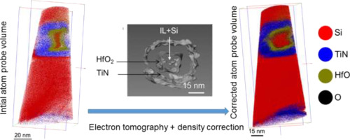
Abstract Atom probe tomography is unique in its ability to image in 3D at the atomic scale and measure composition in a semiconductor device with high sensitivity. However it suffers from many artefacts. The current state of the art of nanoelectronic device analysis by atom probe is addressed and the challenges in device analysis in the next ten years are laid out. Finally the improvements necessary in sample preparation, instrumentation and reconstruction procedures are discussed.
中文翻译:

先进纳米电子器件的原子探针断层扫描:现状与展望
摘要 原子探针断层扫描的独特之处在于它能够以原子尺度进行 3D 成像并以高灵敏度测量半导体器件中的成分。然而,它受到许多人工制品的影响。解决了原子探针纳米电子器件分析的当前技术水平,并提出了未来十年器件分析的挑战。最后讨论了样品制备、仪器和重建程序方面的必要改进。
更新日期:2018-04-01
中文翻译:
先进纳米电子器件的原子探针断层扫描:现状与展望
摘要 原子探针断层扫描的独特之处在于它能够以原子尺度进行 3D 成像并以高灵敏度测量半导体器件中的成分。然而,它受到许多人工制品的影响。解决了原子探针纳米电子器件分析的当前技术水平,并提出了未来十年器件分析的挑战。最后讨论了样品制备、仪器和重建程序方面的必要改进。


 京公网安备 11010802027423号