当前位置:
X-MOL 学术
›
Adv. Electron. Mater.
›
论文详情
Our official English website, www.x-mol.net, welcomes your feedback! (Note: you will need to create a separate account there.)
Room‐Temperature Processing of Printed Oxide FETs Using Ultraviolet Photonic Curing
Advanced Electronic Materials ( IF 6.2 ) Pub Date : 2017-07-12 , DOI: 10.1002/aelm.201600476 Suresh Kumar Garlapati 1, 2 , Julia Susanne Gebauer 3 , Simone Dehm 1 , Michael Bruns 4 , Markus Winterer 3 , Horst Hahn 1, 2 , Subho Dasgupta 1, 5
Advanced Electronic Materials ( IF 6.2 ) Pub Date : 2017-07-12 , DOI: 10.1002/aelm.201600476 Suresh Kumar Garlapati 1, 2 , Julia Susanne Gebauer 3 , Simone Dehm 1 , Michael Bruns 4 , Markus Winterer 3 , Horst Hahn 1, 2 , Subho Dasgupta 1, 5
Affiliation
|
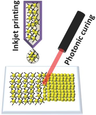
Oxide semiconductors are highly suitable materials for solution‐processed/printed electronics (PE); the growing interest in them can be related to their excellent intrinsic properties, such as high mobility, optical transparency, thermal and environmental stability, and so on. However, high process temperatures remain as the foremost challenge that may limit the compatibility of printed oxide electronics to inexpensive flexible substrates. Here, the possibility of using photonic curing methods to lower the process temperature is investigated, even down to room temperature (RT). Two distinct ultraviolet (UV) curing techniques, involving UV–visible light pulses and continuous‐wave UV lasers are exercised and compared. Combining UV curing with oxide nanoparticulate channel layer and electrolytic gate insulators, it is demonstrated that high performance field‐effect transistors (FETs) with device mobility as high as 12 cm2 V−1 s−1 can be processed entirely at room temperature and realized on plastic substrates. The fabrication steps include printing of a heavily stabilized semiconducting nanoparticulate channel layer, followed by decomposition and removal of the semi‐insulating polymer ligands using UV‐photon energies. The curing process is found to be fast and high‐throughput manufacturing technique compatible. At the same time, the energy requirement to remove the polymer stabilizers is insignificant, thereby ensuring no temperature rise of the parent substrates.
中文翻译:

使用紫外线光子固化对印刷氧化物FET进行室温处理
氧化物半导体是非常适合用于溶液处理/印刷电子(PE)的材料。人们对它们越来越感兴趣的原因可能与它们优异的固有特性有关,例如高迁移率,光学透明性,热和环境稳定性等。然而,高工艺温度仍然是最主要的挑战,这可能会限制印刷氧化物电子产品与廉价柔性基板的兼容性。在这里,研究了使用光子固化方法降低工艺温度的可能性,甚至降低到室温(RT)。对两种不同的紫外线(UV)固化技术进行了比较,它们涉及紫外线可见光脉冲和连续波紫外线激光。将紫外线固化与氧化物纳米颗粒沟道层和电解栅绝缘体结合起来,2 V -1 s -1可以在室温下完全处理并在塑料基板上实现。制备步骤包括印刷高度稳定的半导体纳米颗粒通道层,然后使用紫外光子能量分解和去除半绝缘的聚合物配体。发现固化过程是快速且高通量的制造技术兼容的。同时,除去聚合物稳定剂的能量需求微不足道,从而确保了母体基材没有温度升高。
更新日期:2017-07-12
中文翻译:
使用紫外线光子固化对印刷氧化物FET进行室温处理
氧化物半导体是非常适合用于溶液处理/印刷电子(PE)的材料。人们对它们越来越感兴趣的原因可能与它们优异的固有特性有关,例如高迁移率,光学透明性,热和环境稳定性等。然而,高工艺温度仍然是最主要的挑战,这可能会限制印刷氧化物电子产品与廉价柔性基板的兼容性。在这里,研究了使用光子固化方法降低工艺温度的可能性,甚至降低到室温(RT)。对两种不同的紫外线(UV)固化技术进行了比较,它们涉及紫外线可见光脉冲和连续波紫外线激光。将紫外线固化与氧化物纳米颗粒沟道层和电解栅绝缘体结合起来,2 V -1 s -1可以在室温下完全处理并在塑料基板上实现。制备步骤包括印刷高度稳定的半导体纳米颗粒通道层,然后使用紫外光子能量分解和去除半绝缘的聚合物配体。发现固化过程是快速且高通量的制造技术兼容的。同时,除去聚合物稳定剂的能量需求微不足道,从而确保了母体基材没有温度升高。


 京公网安备 11010802027423号